The record attendance at ECTC a month ago in Dallas was just the latest indicator of the explosion of interest in advanced packaging technologies. The interconnect demands being driven by artificial intelligence (AI) and high-performance computing (HPC) – as well as the broader proliferation of chiplet architectures – is pushing a keen focus today on performance, cost, and sustainability of packaging innovations.
Leading the pack on these metrics for interconnects is a new semi-additive process from Syenta that streamlines RDL and micro-bump fabrication.
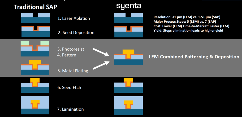
The breakthrough is a process called localized electrochemical modeling (LEM) that combines patterning and electroplating into one process, thus replacing the photoresist application, lithography, and metal plating steps of conventional processes (Figure 1). This simplification reduces infrastructure cost in many ways – equipment acquisition, facility space, energy, staffing, material cost, waste streams – while also reducing the recurring cost with a shorter process time and often a lower layer count and simplified design enabled by finer pitch interconnect.
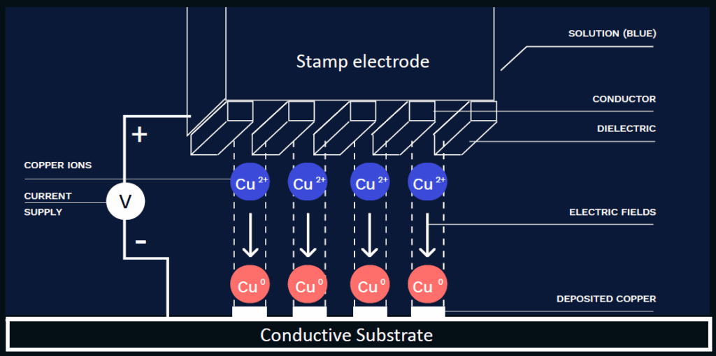
The key innovation of LEM is microscale plating, which uses localized electric fields created by a precision stamp acting as a plating electrode. As shown in Figure 2, the fine features in the stamp create miniature electrochemical cells that allow for very fine control of the plating process. With this approach, both the linewidth and spacing can be reduced. The seed layer for the plating can also be thinner, which is another factor that decreases geometries and reduces process time and cost.
An additional capability enabled with this approach is the option to create variable feature heights by fabricating different groove depths in the stamping tool. This lets the designer optimize RDL layers for better power distribution with thicker lines, for example. Even more flexibility is possible with the ability to deposit multiple material types since the electrochemical cells can be isolated from each other. For example, copper bumps could be fabricated in one area and solder in another area, which can be an important enabler for heterogeneous integration when different IC types with different bond pad metallurgies are being bonded. This would not be possible without extra processing in conventional RDL and micro-bump processes.
Syenta has been doing development work on a lab version of the tool that processes on 10mm x 10mm coupons. Some early results are shown in Figure 3, with serpentine patterns demonstrating the basic process capabilities.
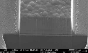
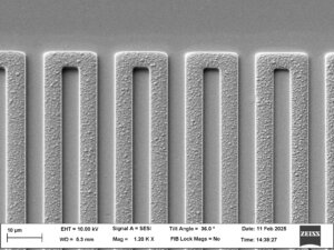
The focused ion beam (FIB) cross-section of Figure 4 shows the thin seed layer and high-quality uniform structure that results from the LEM process.

The Achyon 1 LEM tool was introduced early this year. It is configured for 200mm wafers, a common size for advanced packaging work and medium volumes. Syenta has plans to introduce a 300mm high-volume tool and a panel-level system. The nature of LEM makes scaling up more straightforward than with conventional lithography and plating solutions, so Syenta intends to aggressively push the industry roadmaps. Given the high growth of AI and HPC – which stresses the processor / memory bottleneck – rapid progress in interconnect technology is absolutely critical to keep AI and HPC on track. Syenta is looking forward to being a key driver of these capabilities as the industry surges ahead.