
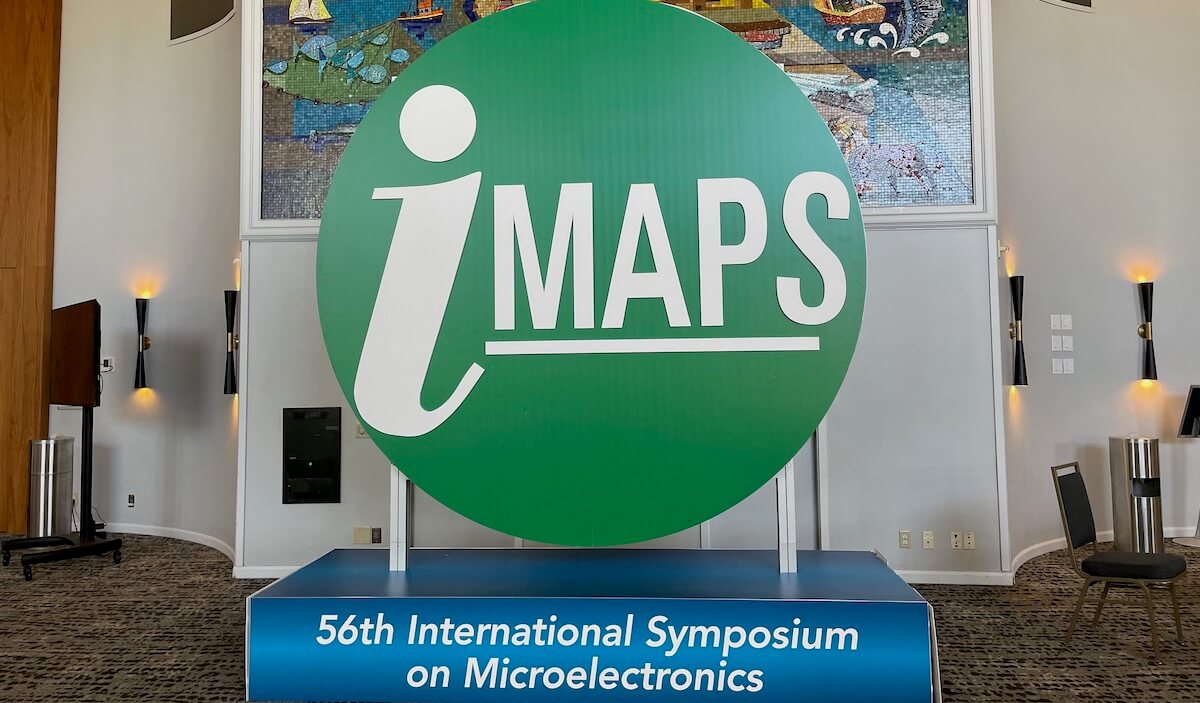
This year’s IMAPS keynotes focused on advancements in heterogeneous integration (HI) technologies and chiplet architectures enabled by HI, driven by the needs of high-performance computing, AI, and automotive applications.
While it feels for some of us that we’ve been in the thick of advanced packaging, HI, and the More than Moore era for a while, the reality is that in the volume manufacturing environment, it is just coming to the forefront. Qorvo’s Kevin Anderson called it “early days” and is excited to see where it’s going to go, and expects “a good, long, exciting career” with it.
Qorvo is a wireless semiconductor supplier that historically is “all about mobile phones” including infrastructure, and WIFI, as well as serving automotive, aerospace, and defense markets. Emerging markets include electrification and green power. Its technology is based in compound semiconductor (III V) materials.
As a “performer” for the US SHIP (state-of-the-art heterogeneous integration and packaging) Program, Qorvo has recently established packaging foundry capabilities with open access in the defense industrial base in Richardson TX, and North Carolina. The goal is to reshore high-volume manufacturing flip-chip advanced packaging.
Additionally, Anderson talked about the advanced technology leg of the project for Qorvo, which involves the development of rigid interposers manufactured from glass or structured silicon to enable larger flip chip die, high I/O density, and embedded die.
From Flip Chip to Interposer
From TSMC’s Shin-Puu Jeng, we learned how interposer technology is a great alternative to flip chips in terms of performance, warpage, chip-package-interconnect (CPI) control, yield, and reliability. He provided a historical look at the early chip-on-wafer-on-substrate (CoWoS) products, and an explanation of how CoWoS allows for reduced spacing between chips to create SoC-like performance.
Jeng continued with a deep technical dive to show the performance advantages of different die-to-die and die-to-high bandwidth memory (HBM) connections. He talked about large-size interposers designed for chiplet integration and shared favorable CoWoS package reliability results. He also gave us a glimpse of the future of CoWoS-R and explained how TSMC is addressing thermal issues for HPC with a package and system thermal solution.
AI Accelerators Enabled By Chiplets
Jeff Burns, IBM, gave attendees a detailed lesson in Deep Learning, and the development of Foundation Models for AI training. Unlike traditional AI models that are task-specific and require labeled data for training, foundation models are trained on large amounts of unlabeled data that can be rapidly adapted to multiple tasks with small amounts of task-specific data.
Unfortunately, it’s very expensive to create these superset foundation models. So, IBM Research is working to democratize AI foundation models using cores and architectures specifically for AI. Burns explained how chiplet integration can hold the key to creating balanced accelerators. Essentially, if you can build FM accelerators using hardened IP functional chiplets, they can be implemented in different ways for different use cases.
![[err-ad-fallback-title]](http://www.3dincites.com/wp-content/plugins/a3-lazy-load/assets/images/lazy_placeholder.gif)
System-level Savings through HI
The final keynote of the week was with ASE’s CP Hung, who talked about electric vehicles (EV) as one of the biggest drivers for heterogeneous integration. Using Tesla as an example, Hung explained how all the different HI technologies have made a plethora of features possible to create a software-defined vehicle that can be updated over the air. He described how these smart, connected vehicles can help optimize the number of vehicles that go through a traffic light, or how EVs themselves can be converted to power sources in case of a power outage.

Hung also talked about the value created by 2.5D and 3D heterogeneous integration at the system level thanks to higher density interconnect, 70% system size reduction, and multiple integration options. This is the underlying philosophy of ASE’s VIPack™.
At the IMAPS Symposium, the company launched its Integrated Design Ecosystem (IDE) a collaborative design toolset optimized to systematically boost advanced package architecture across the VIPack™ platform. ASE’s IDE reportedly enables design efficiencies of up to 50%. In an initial use case for a fan-out chip-on-substrate chip-last (FOCoS-CL) package, the company reports a reduced design cycle time from 90 days to 45 days. Learn more here.
The key takeaway for me was that once again, advanced packaging is proving its value from the early days as a cost adder, as a value add when you consider it from the system level.
For a deeper dive into key takeaways from IMAPS Keynotes check out this week’s podcast below, in which I talk more with Qorvo’s Kevin Anderson, IBM’s Jeff Burns, and ASE’s C.P. Hung.


