

A recent report by Semi Analysis (SA) notes that Intel has backed off on the use of chiplets in its 5th Generation Xeon Scalable Processor Emerald Rapids (EMR).
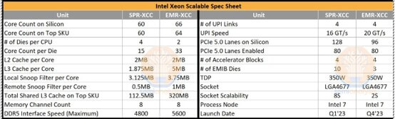
SA reports that at a recent Intel webinar, VP Sandra Rivera revealed that EMR, Intel’s 5th Generation Xeon Scalable Processor, had backtracked on chiplets by designing it using just two large dies. Sapphire Rapids (SPR), its predecessor, had 4 smaller dies, thus they are reducing the number of chiplets from 4 to 2.
The Intel 7 processor will be the basis of the EMR series, which uses its 10nm Enhanced SuperFin technology.
The other major change is that Intel dramatically increased shared L3 cache, from 1.875MB per core on SPR up to a whopping 5MB per core on EMR! That means a top-end SKU comes with 320MB of shared L3 cache across all cores, 2.84x the maximum that SPR offers.
Comparing Sapphire Rapids to Emerald Rapids
SA reports that Intel was able to cram more cores and a whole lot more cache into an even smaller area than SPR including scribe lines, two 763.03 mm² dies make a total of 1,526.05 mm², whereas SPR used four 393.88 mm² dies, totaling 1,575.52 mm². EMR is 3.14% smaller but with 10% more printed cores and 2.84x the L3 cache. This was partially accomplished by reducing the number of chiplets, SA reports that this is not the first time Intel has changed the physical design to save area.
Sapphire Rapids Die Shrink
Intel evidently also did a complete ground-up re-design of Sapphire Rapids since there are two different physical designs and die sizes for the Sapphire Rapids chiplets.
In the numerous silicon revisions done during SPR’s startup, SA identified that Intel changed the physical design and layout of the cores and periphery to achieve a 5.7% area reduction.
The earlier revision had 137 gross dies per wafer while the final version had 148. This required going all the way back to the floor planning and physical design of the chip. One major benefit is that it improved the cost structure of Sapphire Rapids by manufacturing 8% more dies per wafer.
Emerald Rapids
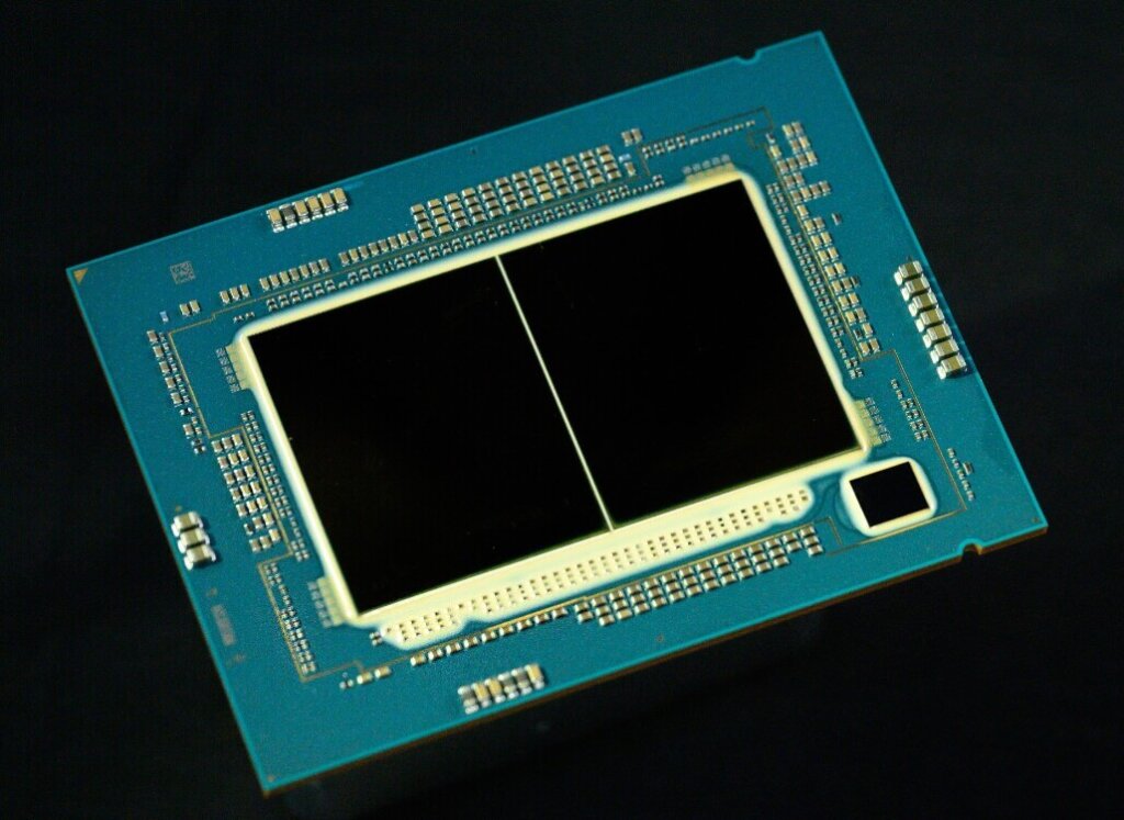
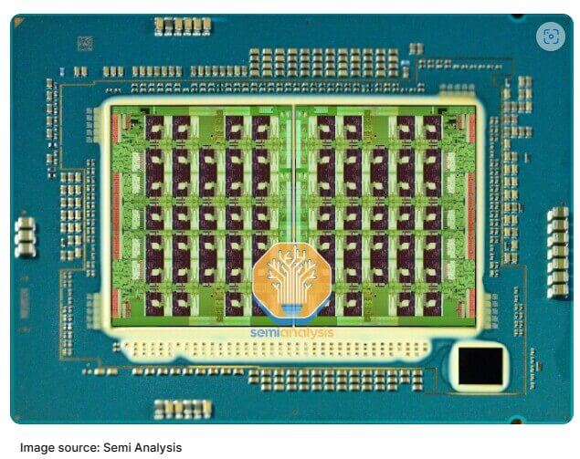
Figure 2 shows the EMR module. Across both dies, the 66-cores plus I/O sections are lashed together on a 7×14 mesh interconnect network.

In the middle, the mesh network crosses the off-chip boundary seven times over EMIB. This compares with the 8×12 mesh across four dies on SPR with 20 off-chip crossings.
The number of silicon bridges has gone down considerably from 10 to just 3, with the middle one being wider to fit three mesh columns. The percentage of total area used for the chiplet interface went from 16.2% of total die area on SPR to just 5.8% on EMR.
Even with all this layout optimization and cramming more cores and cache in a smaller total silicon area EMR is reportedly not cheaper to make than SPR. Despite using less silicon area per CPU, EMR actually costs more than SPR to produce.
Looking at dies per wafer, SA estimates that the EMR-XCC wafer layout matches SPR-MCC, meaning 68 dies per wafer. Assuming perfect yield and die salvageability, EMR could only do 34 CPUs per wafer, down from 37 CPUs per SPR wafer. It gets worse for EMR once factoring in anything other than perfect yields, showing a major disadvantage of going with the larger dies.
Reducing the number of EMIB dies from ten to three would definitely improve packaging costs and yields for the two-chiplet solution. SA concludes by asking “So, if the layout changes and chiplet reduction didn’t help with the cost, then what is the primary driving factor for EMR two-chip solution”
For all the latest in Advanced Packaging stay linked to Insights From the Leading Edge (IFTLE)………………..


