
MUNICH, May 30th, 2023 – ERS electronic, the industry leader in the market of thermal management solutions for semiconductor manufacturing, has developed first-of-its-kind equipment for the metrology and analysis of warped wafers. Thanks to its advanced optical scanning methodology, Wave3000 can accurately measure wafer deformities in specific handling positions. It provides a comprehensive and precise analysis of wafer warpage, which is crucial for ensuring the quality of Advanced Packaging devices.
“With the growing adoption of Advanced Packaging technologies, we see that warpage is becoming an increasingly more complex issue in semiconductor manufacturing,” says Laurent Giai-Miniet, CEO of ERS electronic. “It can be caused by a variety of factors, including differences in material properties, temperature fluctuations, and stress during handling and processing. Warped wafers can cause not only process issues but also production issues leading to defects and reduced yield.”
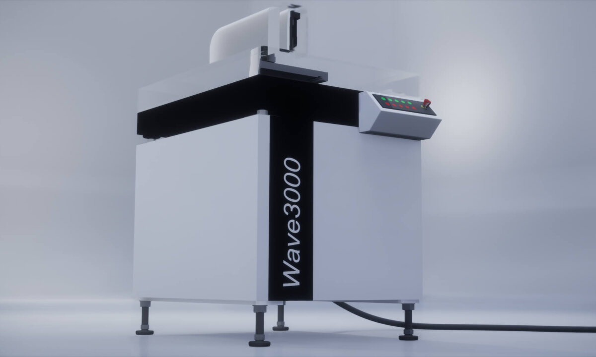
To address this concern, ERS has developed Wave3000, a machine that can measure and analyze warped wafers from 200 to 300 mm with unprecedented precision in less than a minute. The scanner allows the system to measure different wafer surfaces and materials, including silicon, mold compound, and others. Its unique patent-pending measurement methodology offer flexibility by allowing measurements on different platforms, like on pins or on an end-effector.
Post measurement, Wave3000 produces an interactive 3D view of the wafer, which provides a better understanding of the warpage behavior. The 3D view can be rotated and zoomed in, allowing users to view the warpage profile from any angle and assess its impact on the wafer manufacturing process.
“Our new equipment offers a high level of flexibility and precision and can measure warpage, bow, and wafer thickness, which are critical wafer characteristics to avoid yield loss or broken wafers,” says Debbie-Claire Sanchez, Fan-out Equipment Business Unit Manager at ERS electronic. “Wave3000’s advanced software generates an accurate 3D map of the wafer surface, so the user can analyze the warpage impact on the wafer’s performance and make informed decisions on how to optimize process steps for better results.”
This innovation expands the company’s portfolio of automatic, semi-automatic and manual thermal debonding and warpage adjustment equipment for Fan-out Wafer-level Packaging. Wave3000 targets the very large and growing market of semiconductor manufacturers, OSATs, and research institutes working with Advanced Packaging technologies.
Wave3000 is available for purchase now.

About ERS:
ERS Electronic GmbH has been providing innovative thermal test solutions for the semiconductor industry for more than 50 years. The company has gained an outstanding reputation with its fast and accurate air-cool-based thermal chuck systems for wafer probing and its thermal debonding and warpage adjustment tools for FOWLP/PLP.


