

The photo of my May calendar was a picture of a 1956 RAMAC computer with a whopping five megabytes of storage. The note on my calendar states that it could hold the entire phone book of Manhattan. The photo made me think of recent technology announcements, the announcements yet to come in June with the VLSI conference, which discusses advanced technology nodes, and then Semicon West in July where roadmap updates and plans are historically announced.
Nowadays, technology announcements and confirmations that companies are keeping to their roadmaps tend to take place at company events such as TSMC’s technology forum roadshow, and Intel’s upcoming Vision conference. There is still the occasional surprise at conferences such as VLSI, ISSCC, or IEDM, but with logic roadmaps relatively similar over the past technology few nodes, there are fewer surprises. With the recent announcements, and partnerships emerging, I thought I would look at the technology node roadmaps that have been published. It’s been a while since I have seen them side by side so I put them together for review.
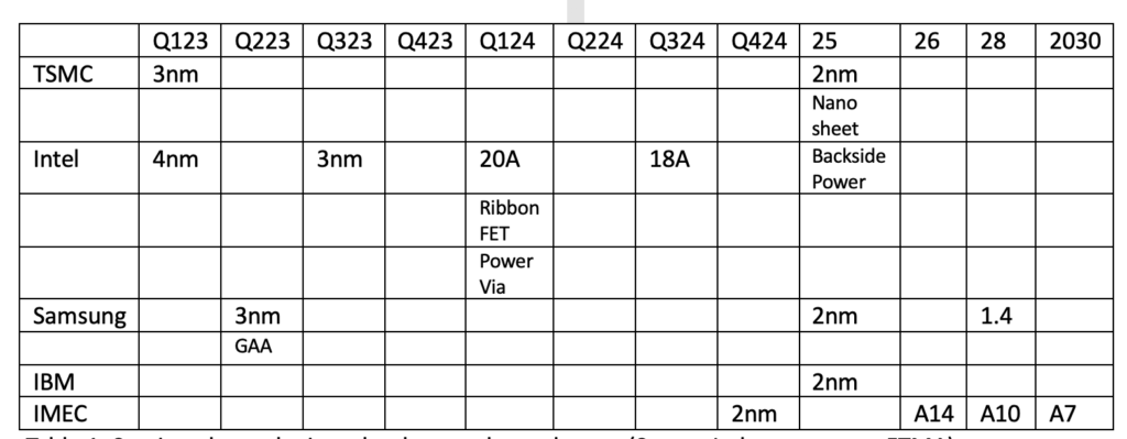
TSMC has been the fast and steady technology node leader since Intel started to lag at 14nm. Under new management, Intel is working to make up ground fast, as you can see from Table 1. TSMC is first to market with 3nm and will most likely manufacture Intel’s first 3nm chip technology the Arrow Lake.
Intel claims to be on track with 3nm processing, so it will be interesting to see when the first 3nm Intel chips roll off the line. Analysts and the industry are not as confident as Pat Gelsinger that Intel will execute to plan. Nevertheless, the company continues to push aggressively down the technology node roadmap.
At its recent technology forum, TSMC presented its roadmap through 2026. No real surprises as TSMC has been very consistent over the years. The one aspect of the roadmap I found to be interesting is the automotive strategy. At 3nm TSMC is giving the automotive manufacturers a bit of a head start on the automotive 3nm technology. TSMC is calling it Auto Early, which gives automakers design rules and SPICE models to design ahead and potentially enables the automakers to have chips tested and qualified when mass production becomes available. It’s also a good marketing plan potentially securing the business early.

According to the comments on their earnings call, Samsung has released its 3nm and is in mass production. The company is working on the second phase of 3nm. So, at the moment two of the three major manufacturers are producing 3nm chips. It should be noted that the Samsung 3nm process is the first gate all around (GAA) or nanosheet transistor, which is quite an accomplishment.
Depending on how you look at the node numbers and interpret the presentations. Intel will be first to 2nm or 20 angstroms, potentially a year ahead of everyone else. Gelsinger says that Intel is currently engaging with customers. Samsung stated that 2nm efforts are going well. And TSMC will be ready in 2025.
IBM, IMEC, and Rapidus expect to be in production with 2nm in 2025. IBM developed the 2nm technology in 2021 and joined forces with Rapidus. Rapidus also signed up to become a core partner in imec’s advanced nanoelectronics technology program. This will be an interesting launch to watch.
IBM used to keep up with Intel and TSMC on transistor development. Additionally, most major logic manufacturers have some sort of relationship with IMEC for pre-competitive technology. They then take it back to their development teams to create the version that works best for their company’s transistor and interconnect design, as well as renaming the technology. Thus, we have names for the transistor like GAA, ribbon FETs, and nano-sheets. The new interconnect technologies are called power rail, power via, and backside power. The variety of nomenclature for technology goes along well with that for nodes, although Intel deviates at 2nm and moves to angstroms, 20A. IMEC does as well beyond 2nm, A14.
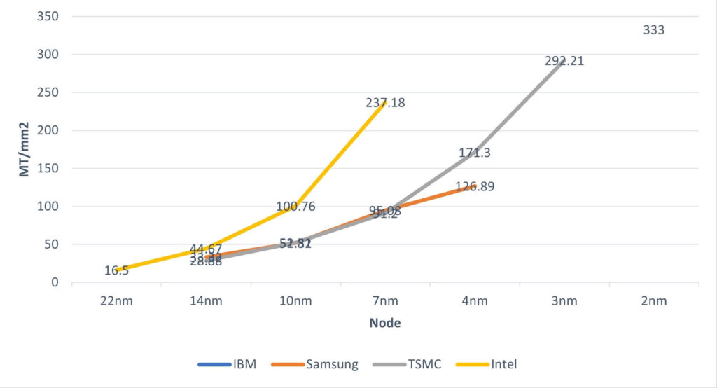
Node naming has been mostly marketing for a considerable time. Ann Kelleher, VP and General Manager of Technology, jokes that we might as well call the technology nodes “George”, as they really don’t mean anything. What gives a bit more insight into who is more advanced in technology are interconnect levels and pitches. Transistor density also gives some insight into technology prowess, as to who can pack more transistors into a specific area. Figure 3 gives a snapshot of the industry shortly after IBM announced its 2nm technology in 2021.

At 3nm, EUV is in production across all companies. The high NA 0.55 EUV tools are expected to be in production first at Intel in 2025. This will likely be for their 18A ramp. The high NA EUV will print features with 16nm pitches. This will hopefully eliminate the need for EUV double patterning for a generation or two.
Most publish roadmaps with numbers, with the exception of IMEC ending at ~2nm. Intel extends to 18A, Samsung to 1.4. IMEC continues down to A2 which they expect to reach in 2036. TSMC presented a more general roadmap, which captures the technology trends needed to continue advancing silicon semiconductor technology, while not placing timeline constraints on the industry.
After tracking Moore’s Law and red brick walls for a long time, I appreciate this approach. This gives the technology direction but the challenges of continuing to shrink, and developing new materials for transistors and interconnects, combined with the need to think sustainably, gives some wiggle room for both technology creativity and sustainability as the industry enters the Angstrom age.


