
While most of us in advanced packaging is familiar with CEA-Leti, CEA-List ( Laboratoire d’Intégration de Systèmes et des technologies) is one of three specialized technological research institutes of CEA specializing in digital systems.
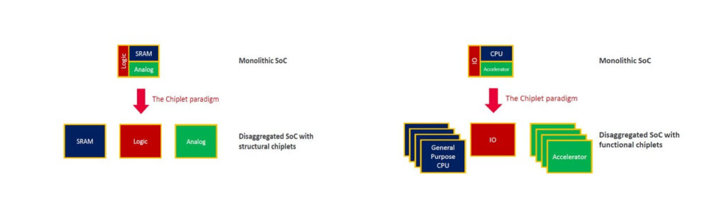
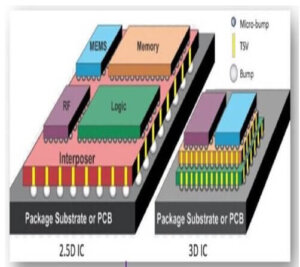
Denis Dutoit, of CEA-List, presentation on “Chiplet Partitioning Can Balance Among Performance, Flexibility and Scalability” at the recent Chiplet Summit. He discussed chiplet partitioning as the new IC design paradigm. I especially liked the slides shown in Figures 1 and 2 for their simplicity in explaining the overall chiplet concept of disaggregation and reaggregation.
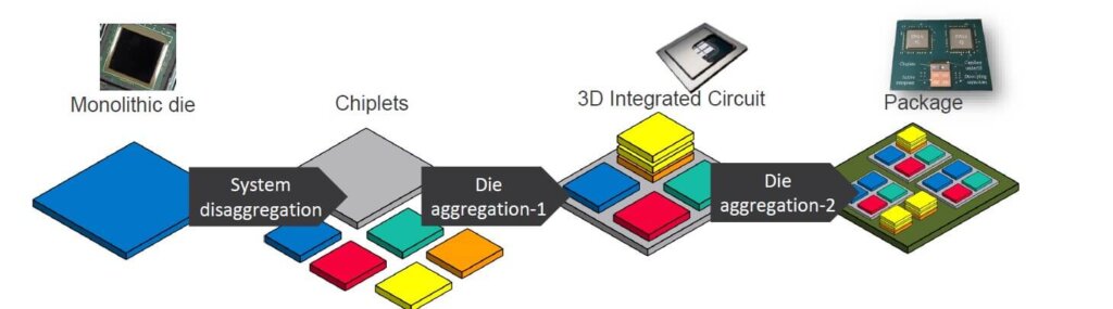
Dutoit explains that system disaggregation consists of both functional and structural partitioning as shown in Figure 2.
Reintegration (reaggregation) requires both advanced packaging technologies and die-to-die interfaces and protocols.
Chiplet Partitioning Needs Heterogeneous Integration
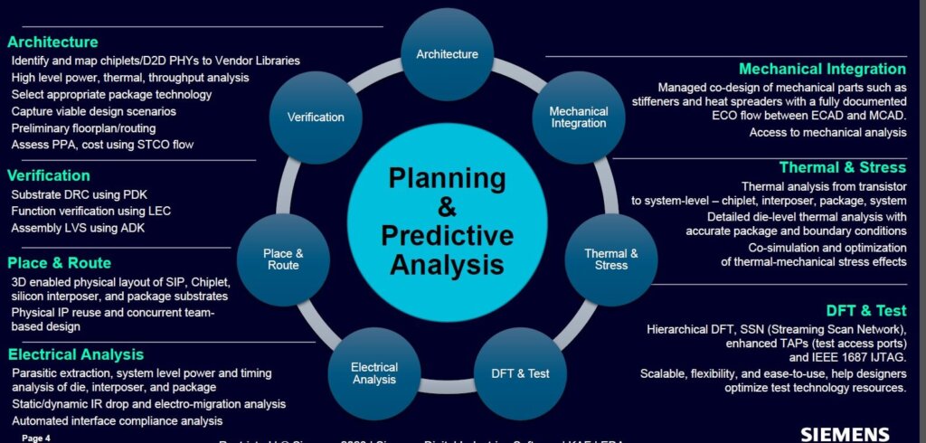
Keith Felton of Siemens EDA discussed “Chiplet-Based Heterogeneous Advanced Packaging” and showed the project flow in Figure 4. He discussed the need to pivot from design-level to system-level optimization. He noted that using chiplets with advanced package brings multiple benefits including:
- Lower wafer costs
- Simpler die/chiplet designs
- Lower power
- IP reuse
- Faster time-to-market
- Better overall system performance
Siemens EDA and CEA-Leti Collaborate on Chiplet Warpage
A joint collaboration between Siemens EDA and Leti shared their thoughts on the impacts of warpage on chiplet-based modules.
Stresses can have both electrical impact (stress impact on the band structure of Si) and mechanical impact (Interconnect fracture – cracking of ULK/ ELK dielectrics, delamination; bump fatigue, and cracking). Stress is unavoidable due to the mismatch of materials’ thermo-mechanical properties. Local stress sources include solder balls and Cu pillars, TSVs, edges of neighbor die, etc.

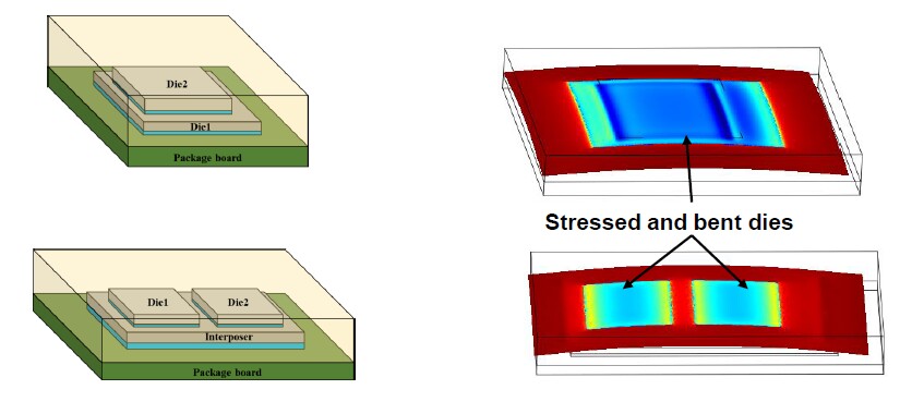
- Combining FEA simulations with layout analysis capabilities allows obtaining chip-package interconnect (CPI) stresses with any desired resolution, by applying a multi-scale simulation technique.
- EDA methodology for assessment of CPI stress impact on circuits performance has been developed by linking stress analysis with SPICE simulations
- For the purpose of mechanical failure analysis in the early stage of a package design, the warpage measurements can be used for the tool’s calibration.
- Analysis of the CPI stress distribution in chip metallization is performed for the estimation of interconnect fracture probability; linked thermal-mechanical simulations – for operational stresses.
DFT for Chiplet-based HI and SiP
Rajesh Pendurkar, from Capgemini (a French consulting company) discussed “DFT (design for test) for Chiplet-based Heterogeneous ICs and SiPs”. He noted the following 3D stacked IC test challenges:
- DFT architectures need to be carefully planned from the bottom up
- Test standards have typically focused on board-level testability (IEEE 1149.1)
- Scan vectors using automatic test pattern generation
- Built-in self-test (BIST) for memory and logic structures
- The importance of known-good die (KGD)
- Package level DFT
- Integration of KGD implementing varying DFT techniques, ie: memory die interfacing with logic die.
- Pre- and post-package test for large and dense arrays of inter die interconnects vertical interconnections using through silicon vias (TSVs)
- Test pattern re-use from constituent chiplets
- IO bandwidth costly repair
- System level DFT
He then told us we should be using the four IEEE test standards 1149.1, 1500, 1687, and 1838 and that system DFT with chiplets requires top-down architecture and bottom-up implementation.
For all the latest in Advanced Packaging stay linked to IFTLE…………………..


