
The semiconductor and microelectronics industries are in the midst of a workforce crisis created by, among other things, the combination of explosive growth and a maturing workforce. Competition for STEM talent in other industries has made it difficult to recruit the latest generation of graduates, who are lured by seemingly sexier opportunities in the end-use application space at companies implementing artificial intelligence, machine learning, augmented and virtual reality, and more.
It wasn’t long ago that semiconductors and microelectronics provided the sexiest opportunities for engineering graduates. Back in the 1960s, that’s where all the exciting developments were happening. And without that early work, we wouldn’t be where we are today. Ask anyone who works in the industry and they’ll tell you that it’s still an exciting place to work today because none of the “cool” devices we use every day would exist without semiconductors and microelectronics.
For this cover story in the 2023 Yearbook, I decided to talk to an industry veteran whose engineering career evolved in lockstep with the microelectronics industry itself, in hopes of inspiring the latest generation of talent to pursue careers in these critical, foundational, and exciting industries.
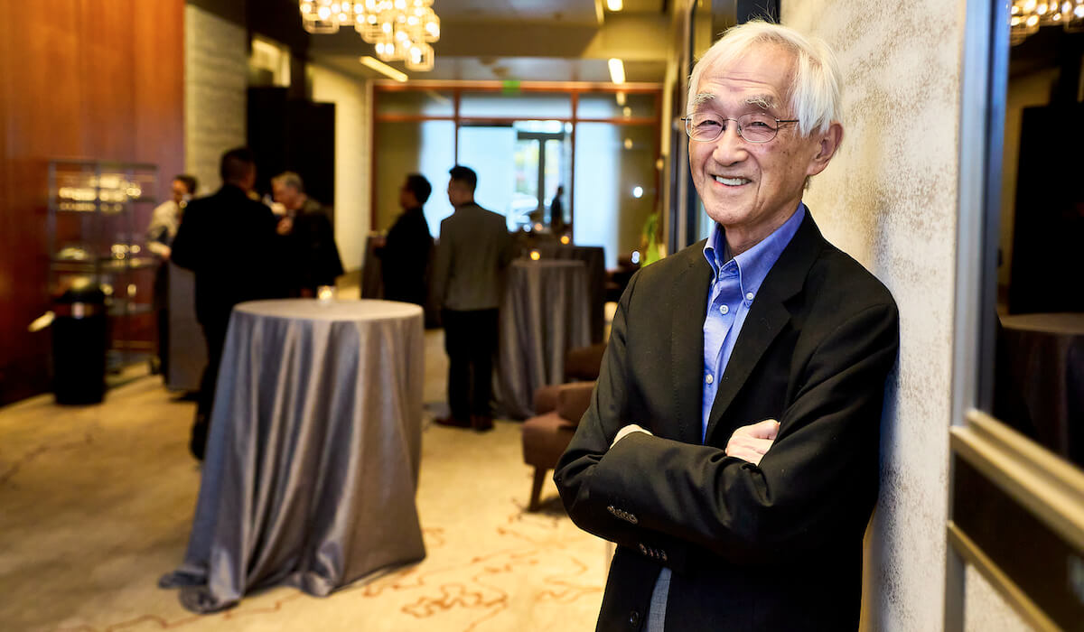
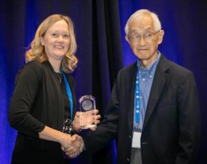
In 2022, Bill Chen, ASE Fellow and Senior Technical Advisor at ASE Group, was awarded The Daniel C. Hughes, Jr. Memorial Award by the International Microelectronics and Packaging Society (IMAPS) for his technical achievements related to microelectronics, combined with outstanding contributions supporting the microelectronics industry, academic achievement, or support and service to IMAPS. I asked him to share his microelectronics journey with us.
Recalling the Early Days
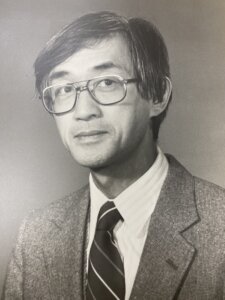
Talking to Bill Chen about his career in microelectronics is like jumping into the pages of a history book. After six decades in the industry, Bill has seen it all, and ridden wave after wave since completing his Ph.D. work at Cornell University, and joining the IBM Development Laboratory in Endicott New York in September of 1963. Endicott was IBM’s birthplace and was the original manufacturing site for computer systems, high-speed printers, and electronic components. That was pre-Moore’s law.
“At that time, both the microelectronic and computer industries were much smaller than they are today,” Bill recalls, “But they were already both recognized as an important part of the global economy.”
Back then, computers were large, bulky, and expensive. They were owned and operated mostly by large financial and governmental institutions. The consumer electronics revolution was yet to happen. People understood that computing advancement was facilitated by innovations in science and technology based on semiconductors and microelectronics.
“While it was a long time ago, it does seem like yesterday,” said Bill.
Choosing His Path
As a newly newly-minted Ph.D. doing his postgraduate course in science and engineering at IBM product development and problem-solving, Bill joined the Advanced Mathematical Science group. The team comprised people with different backgrounds, experiences, and interests. 
“I was an engineer interested in addressing problems in microelectronics. It was a fast-moving field in a fast-moving industry,” Bill explains. “When I joined IBM, I look around to see where my engineering knowledge could be applied and learned how to work together with people from other disciplines and backgrounds. I learned to be creative in addressing engineering issues, posing questions, and how to build on knowledge and intuition.”
Bill also learned that one of the most important things to understand in product development was the product’s design life. This involved knowing which components were most critical, how to test a product design’s robustness, and when sufficient data would be available to confidently launch the product.
“I started to think about how to apply my knowledge to these issues, which lead to a path in engineering,” he said. “I was interested in predictive modeling that starts early in the design phase to understand how things work, how they fail, and how to make them robust enough to last.”
Microelectronics research has been at the core of Bill’s career. While he was at IBM, the company was deeply involved in research and development in everything to do with computers, from integrated circuits to ceramic packaging and printed circuit boards. He found his niche in electronics packaging technologies, supported research across IBM’s global sites, and volunteered at universities.
When the National Technology Roadmap for Semiconductors (NTRS) was first organized, Bill participated in its working groups, as well as when it evolved into the International Technology Roadmap for Semiconductors (ITRS). In 2016, as semiconductor technology appeared to reach its scaling limits, the ITRS published its last edition. As it became clear that the path for continuing along Moore’s Law was in heterogeneous integration through advanced packaging technologies, Bill, along with colleague Bill Bottoms, spearheaded the Heterogeneous Integration Roadmap (HIR), which published its first edition in 2019.
I am very glad that these humble beginning has helped me to contribute to society over the years,” says Bill. “At ASE, my role consists of very little hands-on engineering work and has shifted to being strategic, connecting, advisory, and mentoring. There is great satisfaction in seeing the teams grow in knowledge, strength, and stature, and to see individual engineers and technologists rising to difficult challenges to our complex and expanding electronics industry.”
Being Part of the Advanced Packaging Evolution
For someone like me, who entered the industry in 2005, the term “advanced packaging” has always been part of the microelectronics lexicon. So I found Bill’s perspective enlightening because it extends back to the origins of advanced packaging. He remembers when the shift from gold to copper wire bonding was considered advanced packaging.
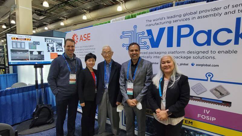
“I was fortunate to be involved when ASE led the industry in copper wire bond development, helping to solve the mysteries of copper wire materials, bonding equipment, and bonding processes,” said Bill. “Now that a sufficient knowledge base and data have been built into industry specifications and test standards, wire bonding is used to package 70-80% of the global semiconductor components. But it is no longer considered advanced packaging.”
Bill explained that like most engineering technologies, packaging technologies have evolved with innovations in materials and equipment developments, as well as in design and architecture. For example, fan-out (FO) technology started with the reconstitution process to address wafer-level chip-scale packaging (WLCSP) components that had insufficient silicon real estate to accommodate required I/O solder balls. Since then, FO technologies have evolved into high-density versions that address multiple-chip integration. It is a highly versatile packaging technology used in leading-edge applications.
“We are still in the early stage of this technology development,” notes Bill. “There will be innovations in design, materials, and assembly equipment as semiconductors move into lower and lower digit nodes and electronics system requirements continue to broaden.” He predicts that FO technology will share the high-performance applications stage with silicon interposers in high-performance computing.
Fan-out is just one part of the heterogeneous integration offering that Bill says is leading to complex packaging integrating multiple chips into a single package, including system-in-package (SiP) and chiplets.

“With heterogeneous integration, innovations across our whole industry is broadening from high-performance computing, data centers and networks to automotive, smart phones, aerospace and defense, medical and health, IoT and the edge,” notes Bill. “At one time the industry was focused on pacing to the next node. Now the market and application spaces are broader and more diverse. The world of heterogeneous integration will be rich with creativity and innovations. The important part for all of us is to bring the whole ecosystem along for the ride.”
Highlights and A-Ha! Moments
It’s not easy to look back over a career that helped a fledgling industry become a global powerhouse and select just a few highlights. For Bill, one of the earliest highlights was gaining recognition for his early work at IBM in predictive modeling, using simulation and modeling verified by experimental design. This proved to be useful in product design from the early conceptual stage to manufacturing.
“While I was very pleased to receive an IBM Division President Award in recognition for my work, it was just as important to hear from a product manager or reliability engineer that the product went through qualification and production smoothly with few technology hiccups,” says Bill.
Fast forwarding a decade or so, Bill says another career highlight, this time when he was at ASE, was working on an eight-year joint development project with AMD to develop and bring to market the first silicon interposer technology.
“While I did very little hands-on engineering work, my role being strategic, advisory, and mentoring, there was great satisfaction in seeing the team and individual engineers rising to the challenges to bring the project to successful fruition,” he recalls.
Most recently, overseeing the HIR initiative has become another career highlight. “This was a collaborative project with many volunteers coming together with a common goal,” He said. “It was truly gratifying to have the HIR released on October 10th, 2019.”
I asked Bill what he tells his grandchildren when they ask about his career. Here’s what he said: “I tell them that what I do is to gain knowledge, and build on the knowledge of many other people before me. And then I endeavor to do good with the whole body of knowledge. The semiconductor industry is exciting and I feel fortunate to have built up knowledge over the decades working throughout dynamic innovation and application cycles.
Advice to Industry Newcomers from Bill Chen
There is no doubt that the world is much more complicated today than it was when Bill Chen first began his career.
“When I started, the microelectronics world and its technology supply chain were much simpler,” he says. “In those days when I had a technical issue that I did not understand it was possible to walk down the corridor to seek out someone and say. ‘tell me what you know,’ and then together walk down to another office and say, ‘Tell me what we should do,’ and then three of us together would collaborate to get the whole technical story together and solution in place.”
Today explains Bill, it’s much more difficult because in the worlds of microelectronics and semiconductors, the technology and supply chain knowledge is much more complicated. “One of the difficulties we have is finding people who understand not just the big picture, but its many detailed parts. That, I think, will be the big challenge,” he said.
Hindsight is 2020
No career is without its challenges. Bill credits his early years at IBM with teaching him how a company works and how all the parts come together. There, he learned how to navigate the inter-company politics that come with working at a large company with a global footprint.
Would he do anything differently?
“Hindsight is 2020,” says Bill. “2022 marked the 75th anniversary of the discovery of the transistor effect. 75 years is a very short time in human history. I am very fortunate to be in this profession at a time when the transistor, semiconductors, and electronics burst into the world. I appreciate the many people who helped me along the way and the many people who had faith in what I do. I cannot thank them enough.”
Bill sees the growing complexities of microelectronics not as a negative, but as an opportunity. He’s excited about the new era of heterogeneous integration. “I’m looking forward to the next decade of advanced packaging, years of heterogeneous integration, years of new devices, new industries, and new knowledge to learn,” he said.
With his finger firmly on the pulse of heterogeneous integration, Bill exudes optimism and passion about the transformative innovation ahead. What could be more inspirational than that? ~ FvT
This article originally appeared in the 2023 Yearbook. Read the issue here.


