

This week we continue our look at the IPC Advanced Packaging Symposium: Building the IC-Substrate and Package Assembly Ecosystem, held in Washington, DC in October. Being the IPC, we could — and should — expect a focus on high-density laminates (HDL) and high-density build-up substrates (HDBU); but they also brought in key US players in the advanced packaging market like Intel, IBM, and AMD.
Intel
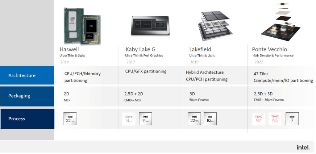
Of interest to IFTLE from a packaging perspective, Tom Rucker gave a presentation focused on Intel’s advanced packaging options, not HDI or HDBU. In Figure 1, you can see how they began to disaggregate (IFTLE prefers “disintegrate”!) systems-on-chip (SoC) into chiplets.
In Figure 2, we see a good reminder of the density increases achievable as we go from today’s standard bumping to tomorrow’s hybrid bonding technology.
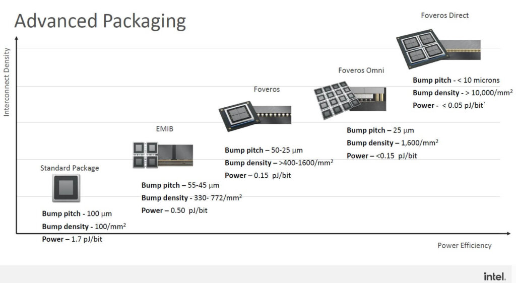
Intel’s Foveros direct (hybrid bonding) is reportedly 16x higher interconnect bump density vs Foveros at 36 µm pitch.
IBM
Dale McHerron of IBM discussed First Level Packaging and Supply Chain Considerations for HPC, focusing on chiplet architectures and the resurgence of the multichip module (MCM).
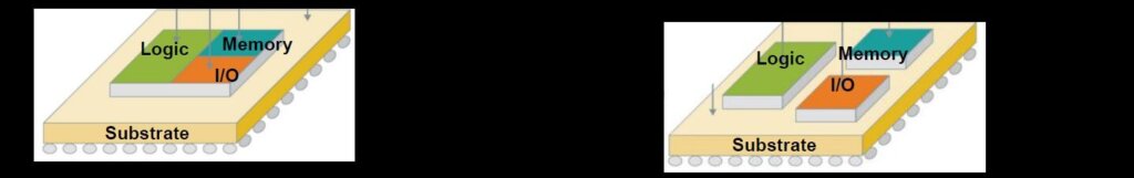
Figure 3 shows his definitions of SoC versus system-in-package (SiP), especially detailing how a SiP can be composed of chips OR chiplets.
McHerron described the drivers for using HI and chiplets for HPC as:
- Node optimization and reuse – design compute, memory and I/O in different nodes for cost and tech optimization
- Die Disaggregation – cost – smaller dies have higher yield; modularity – flexibly compose optimally sized system for application
- Slower Si scaling – node-to-node performance gains are decreasing. We need more Si per mm sq to maintain system improvements
- New workloads – AI is driving the need for memory-intensive computing which requires new architectures for energy efficiency and sustainable growth
When looking at the chiplet platform for HPC and AI McHerron noted the packaging need for:
- Interfaces between components
- High bandwidth (Gbps/mm)
- Energy efficiency (pJ/bit)
- Area efficiency (Gbps/mm²)
- Standards to allow connectivity between a wide variety of components
- Technology Elements
- Scaled interconnects
- Fine-pitch wiring
- Power delivery
- Larger form factors
IBM’s supply chain onshoring recommendations are shown in Figure 4:

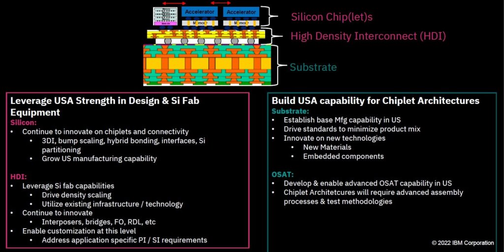
Figure 4: IBM’s supply chain onshoring recommendations. (Source: IBM)
Deepak Kulkarni of AMD gave the company’s advanced packaging presentation showing the traditional, current, and proposed future supply chains. What he sees is:
- More complex supply chain with multiple chiplet vendors
- Chiplets sources from various nodes and foundries
- Chiplet reuse driving common design rules, standards
- Boundaries blurring between fab, assembly, and substrate processes
Figure 5: AMD’s supply chain vision. (Source: AMD)
In terms of HDI/HDBU, they see standardization of design rules processes, and materials to enable multi-sourcing.
For all the latest in Advanced Packaging stay linked to IFTLE……………………..
Find Part 1 of the IPC Advanced Packaging Symposium Here
Find Part 2 of the IPC Advanced Packaging Symposium Here

