Let’s continue our look at papers presented during October’s IPC Advanced Packaging Symposium: “Building the IC-Substrate and Package Assembly Ecosystem”.
NIST and the US CHIPS Act
As we all know by now, the CHIPS and Science Act is being managed by NIST under the Dept of Commerce. NIST has always focused on metrology and has done that job very well. Frank Gayle of NIST gave a presentation entitled NIST, Semiconductors and the CHIPS and Science Act, where he detailed how the operation would be run. The overall spending breakout is shown in Figure 1.
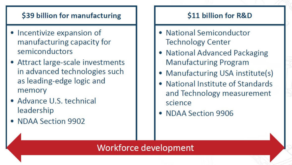
With the following allocation details (Figure 2.)
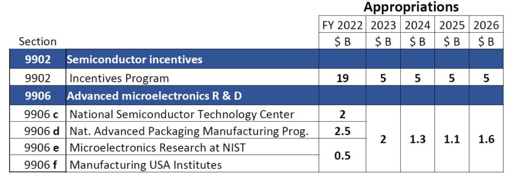
I guess, being run by NIST, it is not surprising that metrology gets a predominant position and NIST gets a significant if not yet fully detailed share of the $11B for advanced microelectronics R&D.
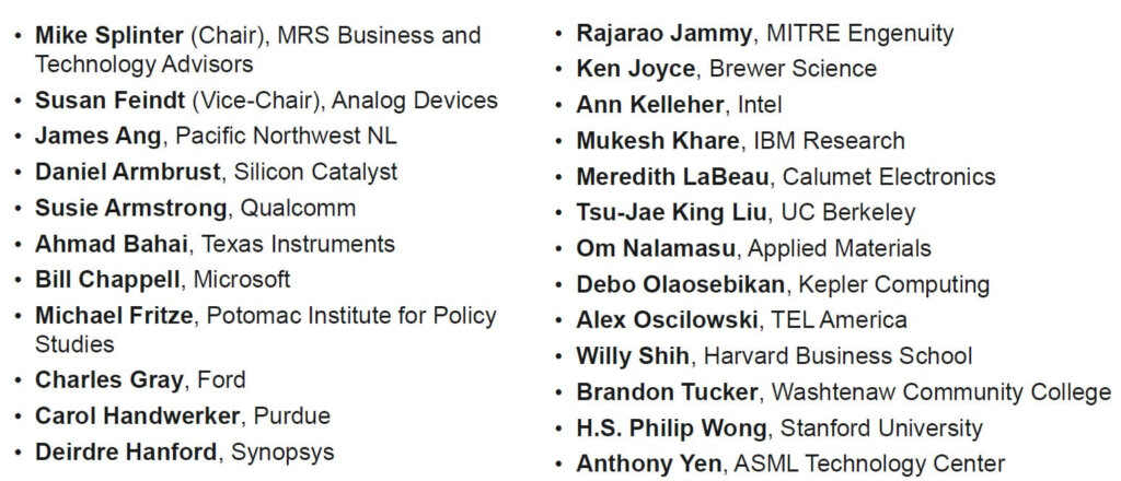
Also of interest, the Advisory Committee has been chosen and is shown in figure 3.
European Commission Chips Act
Francisco Ibanez of the European Commission detailed their initial thoughts on “A Chips Act for Europe”. He noted that EU strengths were seen as R&D, manufacturing equipment, and raw materials, while their gaps included IP and digital design, design tools, manufacturing, and assembly.
If they are calling “R&D”, the presence of their Institutes, then I wholeheartedly agree. I have complained for decades that the US cannot match the capability of IMEC + CEA Leti and the Fraunhofer Institutes. While our universities are great, they simply cannot deliver the capability that comes from these European Institutes and their professional staff. Hopefully the CHIPS Act “manufacturing institutes” will be built to mimic the capabilities of the aforementioned European Institutes.
Northrup Grumman Corp (NGC)
Helen Phillips of NGC detailed the company’s views on advanced packaging for defense applications starting with the comment “ Legacy ceramic, chip/wire packages is being phased out in favor of 2D flip-chip and 2.5/3D advanced packaging”. Priorities for aerospace and defense versus commercial include:
- Truly heterogeneous integration – much more than just silicon
- Maximum performance and SWAP-C driven from the system level
- High-mix, low-volume production
- Stable supply chain over long production durations (decades)
- Reliability, quality, security, and stability throughout the packaging ecosystem and lifecycle
Their assessment of on-shore capabilities is as follows:
Package Substrates
- No Domestic Source
- Dependent on raw materials sole-sourced from Asia
- No domestic capability/capacity
- R&D-level emerging sources only
Wafer post-processing
- Insufficient capability and capacity
- Scattered capabilities require subcontract flows
- Current suppliers can’t meet U.S. capacity or quality
- No non-captive 300 mm Pb bump processing
High-Density Interconnect (HDI)
- Insufficient capability and capacity
- Insufficient capacity to meet U.S. needs
- Limited deployment of advanced materials & processes to meet U.S. targets
- Complex multi-function PWBs high risk
Package Assembly and Test
- 2D: Multiple Sources
- 5/3D: R&D level emerging sources only
- RF Test: Limited complex test capability
Skywater
Chuck Woychick of Skywater reminded us that Skywater is currently bringing up the IMEC silicon interposer technology with BRIDG in Florida and have licensed, and are preparing to scale, the DECA M-Series FOWLP technology and the Adeia hybrid bonding technology at the same site.
Integra
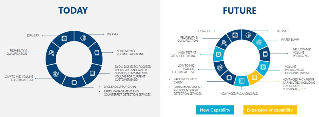
Matt Bergeron of Integra discussed “Trends in SiP and High-speed Substrates and Assembly” They described their business plan as total turnkey manufacturing though nearly all aspects of “advanced packaging” still appear to be in their future (Figure 4).

Its focus is on customers who want to be in the US or cannot go to Asia including:
Trusted, ITAR, military, Aerospace, medical, and quick-turn.
Samsung Electromechanics (SEMCO)
SEMCO gave a presentation on “The Package Substrate Industry: Yesterday, Today and Tomorrow”. There continues to be a significant shortage of package substrates due to sharp demand increases in many areas. Interestingly they report that the Asian supply chain saw no profits from large investments in 2002 and 2012.
They see the following challenges to moving advanced substrate fabrication to North America:
- High ESG cost (environmental regulations)
- High labor cost
- Lack of substrate engineers
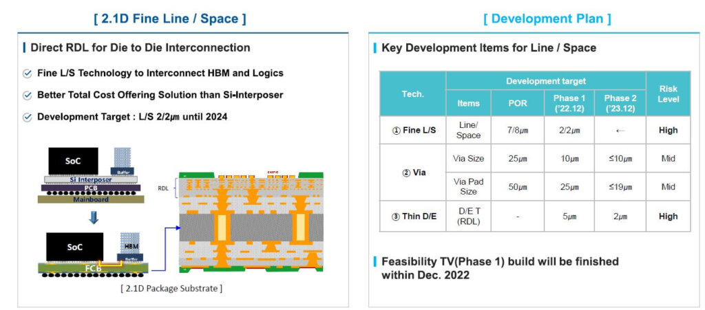
As an example of their latest developments, they showed a so-called “2.1D” laminate package which is scheduled to have 2/2 L/S and 10/19 vias/pads by the end of 2023 (Figure 5).
Need I say, we see nothing like that coming out of the US anytime soon.
For all the latest on Advanced Packaging stay linked to IFTLE…………………..