

IMAPS 2022 Continued…
This year’s IMAPS Symposium in Boston drew 925 attendees and featured:
- 20 technical and poster sessions
- 11 professional development courses
- Keynotes from MIT, Bosch, NXP, Reliance and ADI
- Panel session on mm wave packaging
As always it was a great atmosphere to see old friends and make new ones. Above is an example of an interesting group of senior advanced packaging experts sharing thoughts with President Beth Keser over breakfast.
All in all, IFTLE didn’t see any real breakthrough technologies being presented, but there were many informative presentations.
With all the monies about to be unleashed by the government to bring IC manufacturing and advanced chip packaging back onshore, IMAPS is certainly one of the places you want to be to become part of the advanced packaging community!
So let’s begin taking a look at some of the more interesting presentations.
Mitsubishi Materials Corp
Mitsubishi Materials Corp (MMC) presented an interesting discussion entitled Study for Bonding Technology by Electroplated Nano porous Cu,
Readers of IFTLE are well aware that Cu-Cu direct bonding or “hybrid bonding” is on everyone’s roadmap to become the next advanced packaging interconnect solution (see IFTLE 457: Hybrid Bonding Comes of Age)
MMC pointed out that there are still some difficult operations in such solderless bonding (hybrid bonding) such as control of bump uniformity and the requirement for high accuracy chemical mechanical planarization (CMP). In particular, strict flatness and coplanarity are essential for solderless bonding because there is no liquidus phase during bonding process. The company proposes looking at the use of nano porous (NP) Cu as interconnect materials.
They considered two NP Cu formation processes, de-alloying and direct porous plating. For de-alloying, Cu-Zn alloy bumps were plated, and NP Cu bumps were obtained by de-alloying the Cu-Zn alloy. For direct porous plating process, NP Cu bumps were plated by using unique additives which can form NP structure directly. NP Cu materials have unique properties like softness and lower temperature sintering.
Bonding tests were performed by using NP Cu fabricated by the direct plating method and the de-alloying method. Before the bonding tests, the surface oxide layer was removed by aq H2SO4. After bonding tests, the interface was ion milled and observed by FE-SEM as shown in Figure 1. Defects were observed near the boundary in the case of normal Cu. In the case of NP Cu, defects were well reduced. It is presumed that both the softness of NP Cu and the sintering effect of nano porous promoted the bonding.
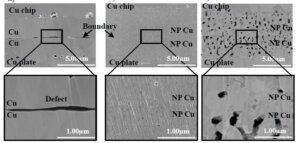
The shear strength of NP Cu was 50-80 MPa while the bonding strength of normal Cu was around 20 MPa. While there is much more work to be done, it is hoped that NP Cu will result in a wider process window for hybrid bonding technology.

Corning Glass’ Adaptive Formed Glass
Corning Korea and KETI (Korean Electronics Technology Institute) discussed Die-embedded Packaging Using Corning Multi-layered Glass.
The presenters propose a packaging solution based on a glass substrate incorporating precisely dimensioned cavities, with a chip positioned in each cavity to prevent them from shifting during processing. Corning Adaptive Formed Glass (AFG), is a laminate glass with a clad/core/clad structure, which allows one to form cavities with high dimensional precision and positional accuracies as well as surface flatness through a described wet etch process. Using a 0.5mm thick AFG they designed and fabricated three types of die embedded packages: single- and double-sided DE packages, and package-on-packages (POPs). High etching selectivity, over 20:1 (in essence the core glass functions as an etch stop) , enabled a wet-etch cavity forming process with accurate cavity depths and flat bottom surfaces (< ± 2.5μm). A double-sided DE package with a total thickness of 600μm was fabricated with two 125μm-thick IC chips, one embedded on each side of the substrate, and connected by metallized through glass vias (TGVs). A POP measured at 5.1×5.1×1.27 mm3 was also successfully demonstrated by using two built-in double-sided DE packages joined by flip-chip bonding, equivalent to stacking four layers of conventional single-sided DE packages
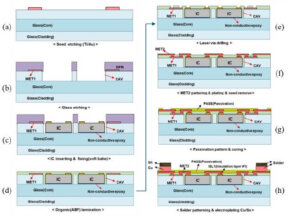
The process sequence for forming embedded die packages is shown below.
They report that the single-sided IC embedded structure showed good via interconnection precision equivalent to existing fan-out packaging technologies.
Unimicron and 2.3D
My old friend John Lau’s presentation State-of-the-Art and Outlooks for 2.3D IC Integration was an excellent review of so called “2.3D” IC integration.
Long-time IFTLE readers know that IFTLE is NOT a supporter of the term 2.3D because it does not clarify what the technology is or does. 2D and 3D are very clear terms. 2.5D, as we have explained to readers many times in the past, was an ASE joke meant to express “we cannot do 3D yet”. Does the community really know what 2.3D physically means especially vs other terms like 2.1D which has also become prevalent. Buttt…as I have also said many times, neither I nor any other individual defines acceptable nomenclature. The community decides what they want to call things and the rest of us simply go along. So… my interpretation of the term “2.3D” is an organic interposer topped with fine line RDL as as shown in the Lau review below.
2.3D can also be defined by the technologies it does not use, namely silicon interposers and through silicon vias (TSVs).
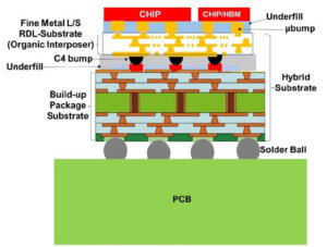
Figure 3: 2.3D IC Integration
Lau does an excellent job reviewing all the technology variations from packaging leaders like: STATSChipPAC, Mediatek, TSMC (InFO), ASE (FOCoS), NEC/Renesas, Amkor (SWIFT), SPIL, Shinko, Unimicron, and I suggest you go back to the original paper to get the original references to further study the differences in these structures.
Lau concludes:
- 3D IC integration is meant to replace the 2.5D IC integration by combining the fine metal L/S RDL-substrate and the build-up package substrate into a hybrid substrate. It is currently in small volume production, and should be in high volume production by the end of 2022. Eventually, 2.3D IC integration will take away some of the market shares from 2.5D IC integration.
- 3D IC integration with fan-out (chip-first) process is simpler and lower cost than that with fan-out (chip-last or RDL-first) process. However, the advantages of 2.3D IC integration with fan-out (chip-last) are: (a) larger die size, (b) larger package size, (c) less die shift issue, and (d) finer metal L/S of the RDLs.
- For 2.3D IC integration with fan-out (chip-last), there are at least two different assembly processes: (a) first bond the chips/HBMs on the fine metal L/S RDL-substrate and then assemble the module (chips/HBMs + fine metal L/S RDL-substrate) on the build-up package substrate, and (b) first combine the fine metal L/S RDL-substrate and the build-up package substrate into a hybrid substrate and test to make sure it is a good substrate, and then bond the chips/HBMs on the known-good hybrid substrate. Due to higher assembly yield, logistic, and less chance to lose the known good die (KGD), the latter assembly process is recommended.
- One can either do chip-bonding first or chip-bonding last. Because of the lower chance of losing KGDs, chip-bonding last process appears to be the superior process.
- Besides the 2.3D IC integration with fan-out packaging technology, there are other 2.3D IC integration structures such as those given by Shinko (coreless substrate), Cisco (organic interposer), Amkor (SLIM), and SPIL (NTI).
For all the latest on Advanced Packaging stay linked to IFTLE……………


