
Every now and then you run across a paper or presentation, and you say to yourself, “This clearly explains this or that technology…this is an important paper”. When I do that, I try to share them with you on IFTLE.
In this case, I’m talking about the paper “2.3D Hybrid Substrate with Ajinomoto Build Up Film for Heterogeneous Integration” presented at 2022 IEEE ECTC by my old friend John Lau and his co-workers at Unimicron.
Now some long-time readers might be saying …” but I thought IFTLE hated the 2.xD terminology?” and you would be right. I was there when 2.5D was introduced in 2009 to the lexicon by Ho Ming Tong of ASE as a joke to explain why ASE wasn’t quite ready for 3D technology (he even chuckled after he said it). It was not meant to be the next buzzword like “nano”, “IoT” or “3D”…but that’s what it became. To then refine that even further with terms like 2.1D or 2.3D is absolutely ridiculous (to me) but I’ll ignore that pet peeve because this was otherwise a great paper.
So, for those looking for a high-density packaging solution without a silicon interposer or TSV, pay attention and go back and read this paper in its full form as presented at the ECTC conference. IFTLE sees such structures as becoming important in advanced packaging in the future.
The Unimicron Process
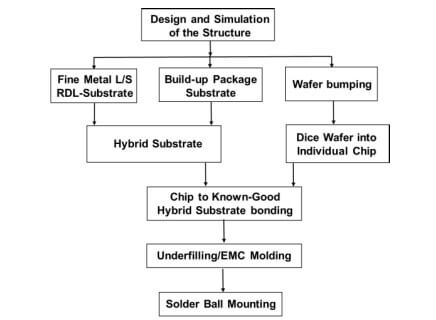
The flow chart for the technology we will be describing is shown in Figure 1:
A cross-section of the final structure is shown in Figure 2:
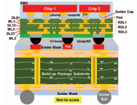
The two chips are supported on the “hybrid substrate”, which is fabricated by combining the thin film RDL-substrate (20mm x 15mm x 53μm) and the build-up package substrate (23mm x 23mm x 1.3mm). The interconnection between the thin film RDL-substrate and the build-up package substrate is through C4 solder joints and underfill (Figure 3).
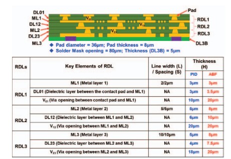
There are 3 RDL layers, each consisting of a dielectric layer and a Cu metal layer. The DL material y is an ABF film that is cured at ~ 200°C. The L/S of RDL1 is 2μm/2μm, of RDL2 are 5μm/5μm, and of RDL3 is 10μm/10μm. All the vias between the metal layers are 20μm (Figure 4).
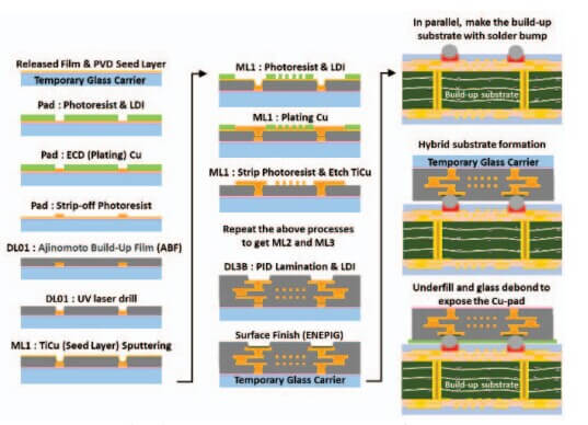
A 1µm sacrificial release film is slit-coated on a temporary glass panel and then a Ti/Cu seed layer is PVD deposited on top. The contact pad can be defined by photoresist, laser direct imaging (LDI), development, and ECD Cu. Then a 12.5μm ABF film dielectric layer is cured onto the plate. The first dielectric layer is drilled by a UV laser to obtain the blind vias. It is followed by Ti/Cu PVD, photoresist, LDI and development, Cu ECD, strip off the photoresist, and etch off the TiCu to obtain the first metal layer. Subsequent dielectric/metal layers are obtained by repeating the same process steps. The 5μm-thick solder mask passivation is obtained by laminating a 10μm ABF dry film and LDI. Then, the surface is finished with electroless Ni / electroless palladium/immersion gold (ENEPIG) completing the thin film substrate.

The “hybrid substrate” is completed by assembling the thin film RDL-substrate and the build-up package substrate with C4 solder bumps.
The dimensions of the test chips are 10mm x 10mm x 150μm and 5mm x 5mm x 150μm. The minimum pitch of these chips is 50μm. Both chips have Ti/Cu (0.1/0.2μm) UBM AND 32μm-diameter pads, the Cu-pillars are 32μm-diameter and 22μm-tall, and the SnAg solder cap is 15μm with a 3μm Ni barrier.
Extensive finite element analysis by Unimicron demonstrates that the hybrid structure should be reliable for most operating conditions. Reliability tests are ongoing…
Will such structures pass all standard reliability tests and yield on full 500 x 500 glass panels? We will see.
For all the latest on Advanced Packaging stay linked to IFTLE……………..


