

CHIPS and Science Act
The CHIPS and Science Act will provide $54.2B in funding for the semiconductor and wireless industry, including $52 billion in grants and incentives specifically for the American semiconductor industry. In addition, a 25% investment tax credit for the manufacture of semiconductors and tools to create semiconductors will be included, alongside $500 million for an international secure communications program, $200 million for worker training, and $1.5 billion for public wireless supply-chain innovation (source: BGR Group).
I must admit that IFTLE, not being in the least bit trusting of anyone in the political realm, is worried that the name change (the addition of “and science”) was done to allow everyone’s pet projects into this legislation since when you come down to it, most things can be linked to “science”.
So….with fingers crossed, here is a nice description of the CHIPS and Science Act funding from the BGR Group.
CHIPS Act – ($54.2 billion)
Commerce Department Incentives Program ($39B)
The incentive program would have $39B allocated to implement the Semiconductor Initiative Program Financial Assistance Program (FY2021 National Defense Authorization Act Section 9902), which requires the Commerce Secretary to establish a program that provides financial assistance to incentivize investment in semiconductor facilities. Within the incentive program, up to $6B may be used for the cost of direct loans and loan guarantees.
Advanced Microelectronics Research and Development ($11B)
This $11 billion should be allocated to several programs including the National Semiconductor Technology Center (NSTC), National Advanced Packaging Manufacturing Program, and other R&D and workforce development programs. The FY22 funding would include $2B for NSTC, $2.5B for advanced packaging, and $500MM for other related R&D programs. Funding for FY23-FY26 to be used across the programs would include $2B in FY23, $1.3B in FY24, $1.1B in FY25, and $1.6B in FY26.
CHIPS for America Workforce and Education Fund – ($200M)
- CHIPS for America Defense Fund – ($2B)
- CHIPS for America International Technology Security and Innovation Fund – ($500M)
- Public Wireless Supply Chain Innovation Fund – ($1.5B)
Appropriate $1.5B for the Public Wireless Supply Chain Innovation Fund with the goal of encouraging movement toward open-architecture, software-based wireless technologies and funding innovative technologies in the U.S. mobile broadband market.
Advanced Manufacturing Investment Credit
This is a 25% investment tax credit for semiconductor manufacturing investments and includes incentives for the manufacturing of semiconductors and specialized equipment required in the semiconductor manufacturing process. This credit begins after 12/21/2022, for properties for which construction begins before January 1, 2027.
TSMC Phoenix “…on time and on track”
DigiTimes Asia reports that TSMC is “is on time and on track” concerning the construction of Fab 21, its new 5nm fab in Phoenix.
They report that TSMC is scheduled to begin equipment move-in in the second half of 2022. They expect to enter volume production (designed for a capacity of 20,000 wafers/month) in the first quarter of 2024. TSMC chairman Mark Liu revealed higher than expected costs for the new fab and said subsidies from the US Government would be vital to TSMC’s efforts to reduce costs.
The feature photo above is an artist rendering of the entryway of TSMC campus in North Phoenix. Source: AZ Central and TSMC.
Apple 20-core M1 Ultra processor
In IFTLE 518 we discussed the Apple M1 Ultra processor.
Earlier in the year, it was rumored that Apple was going to use TSMC’s CoWoS-S (chip-on-wafer-on-substrate with silicon interposer) 2.5D interposer-based packaging, which is a proven technology used by a number of companies. In IFTLE 518 we quoted Dick James from TechInsight, who felt from analysis of the cross sections that this was a CoWoS – L solution, though he did say there was an “…outside chance that it was InFO-L.

According to recent reports from Toms Hardware blog that is not correct (Figure 1).
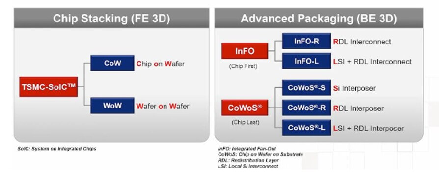
Reportedly TSMC showed a slide at the International Symposium on 3D IC and Heterogeneous Integration” (held in late April at Hong Kong University), indicating that Apple is using Integrated Fan-Out (InFO) with local silicon interconnect (LSI) and a redistribution layer (RDL), i.e. InFO-L.
InFO-L uses localized silicon interconnects beneath multiple dies instead of full silicon interposers, similar in concept to EMIB. Evidently, since Apple is not using HBM memory stacks and does not need to integrate dies that are larger than interposer, InFO meets its needs.
TSMC Slows down 3nm Chip Production
TSMC says it has decided to slow down its 3nm chip production as Intel, one of its major customers, announces plans to push back the launch of its new Meteor Lake GPU chipsets to the end of next year.
Based on Intel’s original schedule, TSMC was to start producing the new chipsets in the second half of this year. The postponement would leave Apple as the only customer for the technology for the next one-and-a-half years. Other announced major customers for TSMC’s 3nm technology, including AMD, MediaTek, and Qualcomm, in 2024.
The Intel order cuts could lead to a reduction in TSMC capital spending for next year, given that 3nm equipment will not be put in place before it is needed. To avoid booking hefty depreciation and amortization costs for the new 3nm equipment and idled capacity, TSMC has reportedly notified its equipment suppliers about the order adjustments for next year.
For all the latest in Advanced Packaging stay linked to IFTLE…………………


