
Apple announced that it’s launching the new M1 Ultra processor for high-end Macs during its ‘Peek Performance’ event in March and announced the mysterious “UltraFusion” as Apple’s “custom-built packaging architecture.” Let’s take a closer look!
Is Apple M1 using TSMC CoWoS technology?
The Apple M1 Ultra is currently only available inside the new Mac Studio, which is a workstation desktop PC with a similar (but larger) design to the Mac Mini. It claims the M1-Ultra-powered Mac Studio provides CPU performance up to 3.8 times faster than the 27-inch iMac with a 10-core processor.
The M1 Ultra shares the same 5nm architecture as previous Apple M1 processors but has 20 CPU cores and 64 GPU cores making the Ultra the most powerful chip that Apple has ever produced. Apple suggests the M1 Ultra is 7x more powerful than the standard M1 chip.
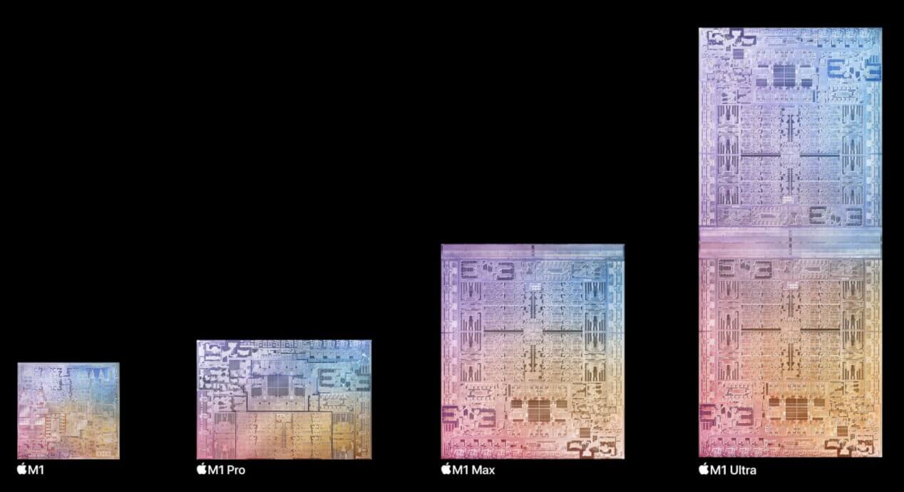 Figure 1: Apple’s M1 family.
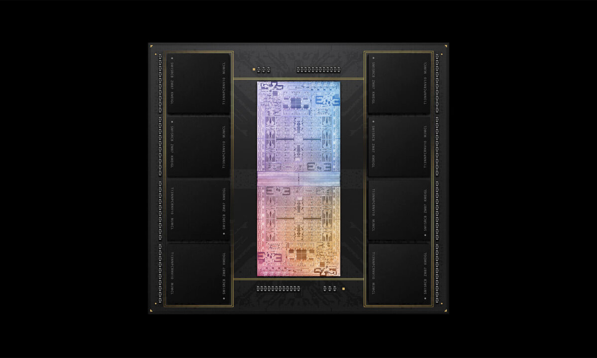
The UltraFusion technology used by Apple allows the two M1 Max chips to connect over 10K signals and maintain an inter-processor bandwidth of 2.5TB/s.
The new system-on-chip (SoC) consists of 114 billion transistors, done in TSMCs 5nm process node, the most ever in a personal computer chip. M1 Ultra can be configured with up to 128GB of high-bandwidth, low-latency unified memory that can be accessed by the 20-core CPU, 64-core GPU, and 32-core Neural Engine.
At twice the size of an M1 Max, the M1 Ultra consumes about twice the power and throws off twice the waste heat, a big design constraint for computers.
UltraFusion is rebranded CoWoS from TSMC
To build M1 Ultra, the dies of two M1 Max are connected using what they are calling “UltraFusion”. Well, it ends up there is no new technology involved. Ultrafusion is a rebranding of supplier TSMC’s CoWoS technology.
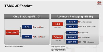
Let’s refresh our memories with the following descriptions of the TSMC advanced packaging “fabric” which we learned about in IFTLE 464.
So…. we are talking about their CoWoS technology, but the question is which one?
Techspot (via reports from Digitimes Asia) has reported that “It is believed that Apple chose CoWoS-S (what we used to call a simple 2.5D silicon interposer) over InFO-LSI as the latter was not ready in time for the M1 Ultra. So, Apple might have played it safe by opting for a proven but more expensive solution over a cheaper, more nascent technology”…

You may recall that InFO-LSI (InFO with Large Scale Integration (LSI) is a newer alternative to CoWoS-S in TSMC’s technology options for ultra-high bandwidth chiplet integration. InFO-LSI uses localized silicon bridges vs full silicon interposers, similar to Intel’s EMIB (embedded die interconnect bridge). If this is correct, IFTLE would expect that one would logically expect a move to the lower cost InFO-LSI in the next M1 generation.
FYI – Digitimes reports that Unimicron is supplying the substrate with ABF RDL.

On the other hand, my good friend Dick James at TechInsights, who has done reverse engineering on many of the world’s most important packaging technology in the past few decades, reports that it is more likely Apple will go with the TSMC CoWoS-LSI solution where an “LSI” Si bridge is joining the two M1 chips as shown in Figure 3.
The M1 Max is ~ 19x 22mm, or ~420mm2, so a TSMC CoWoS-S-style interposer would be a minimum of 840 mm2, right at the reticle limit. That’s a lot of expensive silicon. He also points out that the Apple press pictures (Figures 4) look more like they are trying to depict a silicon bridge vs a full silicon interposer.
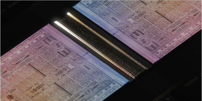
James also reports that the bump pitch shown in Figure 5 is 25µm.

James also offers that there is an outside chance that this is a specialized InFO-L package from TSMC.
In any case, the Apple studio with the M1 Ultra will be available on March 18, so we do not have to wait much longer to understand what “UltraFusion” really is.
For all the latest in advanced microelectronic packaging stay linked to Insights From The Leading Edge (IFTLE)!


