
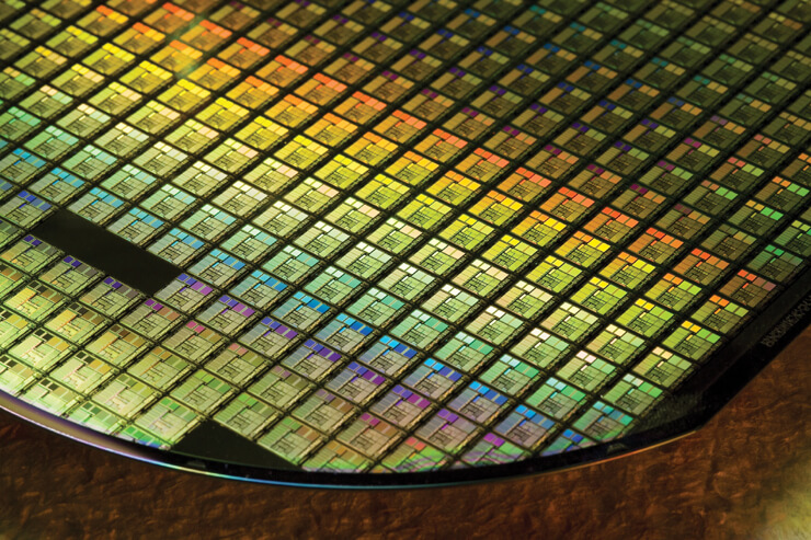
TSMC 2nm Chips Coming in 2025
At its recent North America Technology Symposium TSMC announced that it will begin volume production of 2nm chips by 2025. TSMC’s roadmap is similar to that of its major competitors—Samsung and Intel—which also have reported also have plans to manufacture 2nm chips around 2025.
TSMC reports the 2nm chips will be 10-15% faster at the same power or save 25-30% power at the same speed compared to its 3nm process. The 2nm chips will feature a new technology called “nanosheet transistor architecture” TSMC said. TSMC has said it will build the initial 2nm wafer plant in northern Taiwan’s Hsinchu and later expand production to Taichung in central Taiwan.TSMC launched the 5nm process in 2020 and is scheduled to start commercial production of the 3nm process later this year.
Samsung Announces 3nm Process
Samsung Electronics reports that it is planning to catch up with Taiwan’s TSMC, by establishing a 3nm GAA (gate all around) process within the next three years.
GAA is a next-generation process technology that allows a gate to contact all four sides of a transistor, versus the three sides in the case of the current FinFET process. The GAA structure can control the electrical current more precisely than the FinFET process.
Samsung reportedly started pilot production of the 3nm GAA process in early June, becoming the first company in the world to use GAA technology. The 3nm process reportedly boosts semiconductors’ performance and battery efficiency by 15% and 30%, respectively, while reducing chip areas by 35% compared to a 5nm process.
Samsung reports plans to introduce it to second-generation 3nm chips in 2023 and mass produce GAA-based 2nm chips in 2025. TSMC’s strategy is to enter the 3nm semiconductor market in the second half of this year using a stable FinFET process, while Samsung Electronics is betting on GAA technology. TSMC is expected to introduce a GAA process beginning from 2nm chips and release the first product around 2026.
Business Korea reports that TSMC originally planned to mass-produce semiconductors for Intel and Apple with 3nm technology beginning in July of this year, but is having difficulties obtaining sufficient yield. NVIDIA paid TSMC up to US $9B in advance for production of the GeForce RTX40 GPU series, to be released within this year, using a 3nm process, but will receive 5nm products instead of 3nm products. They report that TSMC had difficulties in securing a desired yield on the 3nm process and has consequently revised its technology roadmap several times.
A similar situation is facing Samsung Electronics. Wafers were put in for pilot mass production in the 3nm process, but the company has been putting off its official mass-production announcement due to a low yield problem.
Who Will Lead in the Next 5-10 Years?
While the Big Three (Samsung, TSMC, and Intel) continue to expand their share of the pie, Digitimes has looked at the question of “Who will be Leading in the Next 5-10 years?”
Digitimes expects TSMC to pass Intel in revenues in 2023 as shown in Figure 1.
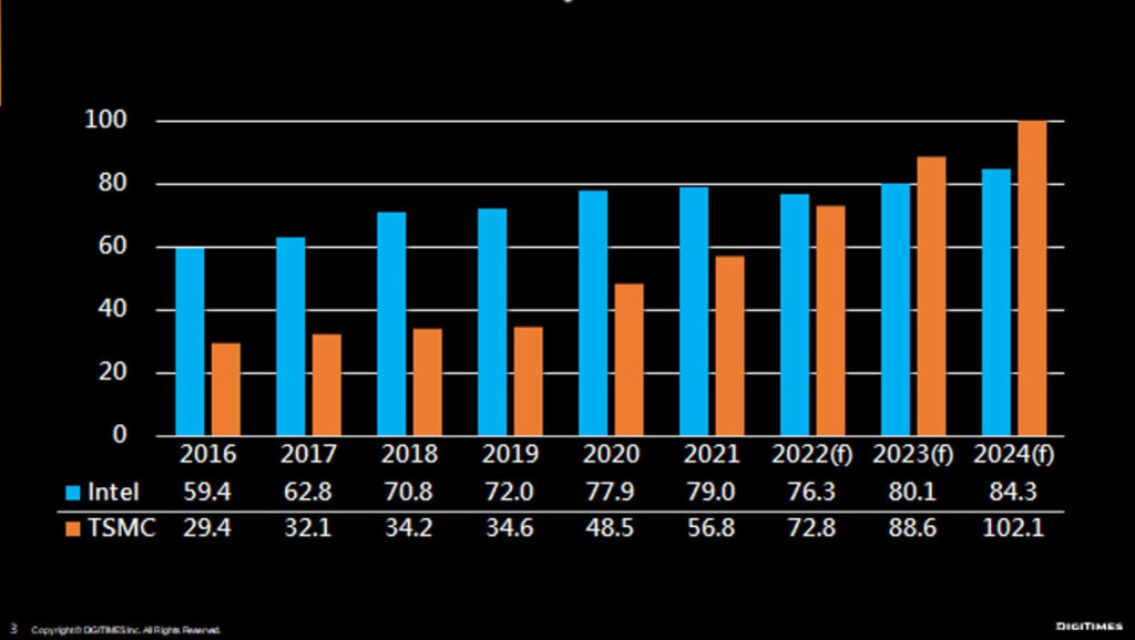
Figure 1: Projected revenue comparison of Intel and TSMC, compiled by DIGITIMES, May 2022
Samsung is currently the industry revenue leader with DIGITIMES estimates of $82B in 2021, with memory accounting for 77% of the total and the remaining $18.77B from System LSI, which offers foundry services for logic ICs.
But TSMC now invests 60% of its revenue in capital expenditure, which is almost impossible for Samsung. Digitimes reports that TSMC is the only company in the world that uses CAPEX as a strategic weapon.

If Samsung were to try to equal TSMC’s CAPEX by using revenue from their memory business, it would be 180% of Samsung’s non-memory revenue, which is not a logical business decision. Therefore, Digitimes reports it expects TSMC to lead the big three in revenues over the next 5-10 years.
Advanced Packaging Becoming a Powerful Industry Segment
IFTLE reported to you more than a decade ago that TSMC had its sights on advanced packaging as a means to gain more IC business. It is now well accepted that advanced packaging technology has become a powerful tool for TSMC to grab orders for advanced chips.
Digitimes says it believes that the back-end advanced packaging business of TSMC has been a key to their obtaining Apple orders vs Samsung. TSMC’s back-end plant is located in Longtan ( northern Taiwan) and is considering setting up a new plant in Chiayi or Yunlin in southern Taiwan to expand production capacity
We now hear that Samsung Electronics has also announced that it will strengthen its back-end packaging and testing technology by establishing a new semiconductor package process organization. This is a strategy to gain competitiveness in the post-processing sector which they have been falling behind TSMC.
The Samsung TP Center is expected to become the spearhead vanguard of semiconductor packaging and test at Samsung. Recently, packages and tests became the core characteristic that determines the competitiveness of a semiconductor.
The top 10 OSATS revenue in 2021 reached $33.7B and they accounted for 90% of the overall market. Taiwan’s packaging and testing industry are worth $23.2B, or 58% of the global output value, followed by China with $9.5B or 24%.
They question, “Will second-place Amkor be put up for sale?” Amkor, a US-based firm, is an important part of the industry but has no production capability onshore in the US. The packaging and testing industry is relatively fragmented geographically, with Malaysia, Thailand, and the Philippines hosting major hubs.
For all the latest on Advanced Packaging stay linked to IFTLE…………………….


