
Another Heterogeneous Integration Roadmap
The UCLA Center for Heterogeneous Integration and Performance Scaling (UCLA CHIPS) and SEMI have announced that they have been awarded a $0.3MM grant from NIST to produce a roadmap for advancing heterogeneous integration and advanced packaging technologies in the US. This is one of the first awards by NIST’s Advanced Manufacturing Technology Roadmap Program, and will fund the project for 18 months.
We are told in press releases that “the roadmap will build upon the previously established International Technology Roadmap for Semiconductors (ITRS)” and that SEMI, the global electronics industry association will “…define a process for prioritizing and guiding critical areas of the HIR to standardization” and UCLA CHIPS will “…organize academically themed workshops and panels to ensure the roadmaps are scalable and extendable as new applications evolve and new processes are developed”…but if you’re like IFTLE you’re saying “exactly what does that mean?”
To get a better understanding IFTLE took a look at the presentation Professor Subu Iyer gave at the HIR meeting at the recent IEEE ECTC conference in San Diego. The following information is taken from that presentation:
Let me start with the conclusions first:
- Microelectronics is now recognized as strategic to the US economy
- Packaging is now recognized as strategic to microelectronics
- The is almost NO on-shore package manufacturing in the US
- We need to change this!
Professor Subu Iyer (ex-IBM), Director of the UCLA Center states that their goal is to “translate the HIR into a blueprint for onshore manufacturing that can drive materials, equipment, manufacturing processes, supply chain and product manufacturing with a trained workforce in the USA.” They intend to draw from existing HIR working groups where appropriate and create a few new working groups from other organizations for non-HIR covered areas.
Looking at the 2021 HIR roadmap they view chapters 1-7 and 12 as application-driven; chapters 8-11, 15, 16 20-24 as technology-driven; chapters 13,14 as design-driven, and chapters 18 & 19 as ecosystem driven. They will try to consolidate these chapters into actionable manufacturing plans.
Additional topics to be included:
- Sustainable manufacturing
- Standards: electrical, mechanical, equipment, traceability, data management
- Workforce development: on-the-job, college, HS, vocational schools, etc.
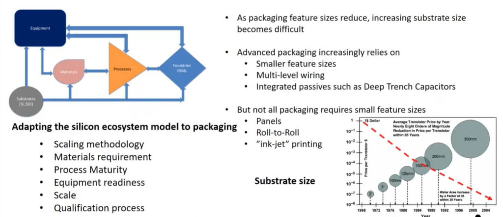
They will attempt to apply the silicon ecosystem model to packaging as shown below. Iyer asks “What will our scaling technology for packaging be?”, i.e similar to Moore’s Law for IC fabrication. In packaging, we see a trend towards customized manufacturing where you make small changes in the manufacturing process to adapt to different applications. So, Iyer asks, “How do we mimic silicon scaling while developing customizable packaging?”
Iyer notes that going to larger-size wafers was the main driver for silicon technology, i.e. going from 200 to 300mm but that could only go so far. There was also an attempt to go to 450mm but it fell apart because it became very clear that it was not possible to increase the wafer sizes due to equipment constraints. Iyer poses the question for advanced packaging “…is it necessary to have very large substrates (panel processing) or should we be focused on throughput?” Iyer claims to be skeptical about going to large panel sizes but knows others think it can be done. In either case, Iyer thinks this must be addressed and answered (Figure 1.
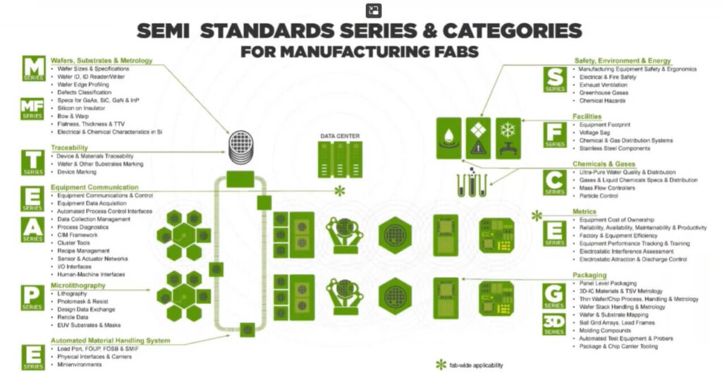
Everything in the silicon industry is standardized (Figure 2). It is logical that similar standardization needs to be undertaken by the packaging community.

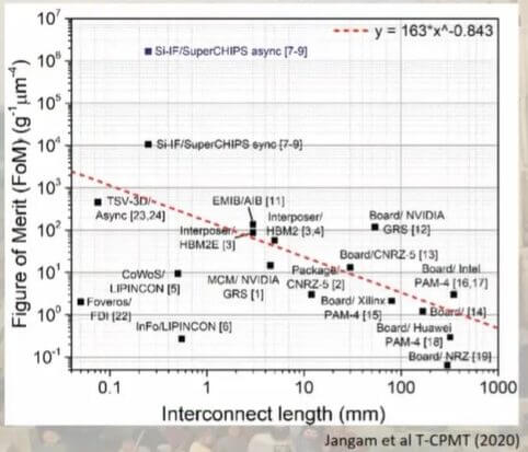
Communication between chips also needs to be addressed. Iyer described today’s situation as a “tower of Babel.” (Figure 3)
As IFTLE readers know, we are currently trying to standardize chiplet-to-chiplet communications (see IFTLE 517) and Iyer indicates that more of this needs to be done. As IFTLE readers know IFTLE has been pushing for packaging standardization since its inception 500+ blogs ago…
UCLA/SEMI Roadmap Timeline:
- Kick-off meeting by June 30th
- Monthly virtual meetings with TWG leaders
- Workshops every 6 months
- Final report to NIST Feb ‘24
China orders the Government to Replace Foreign Computers
The Taipei Times reports that China has ordered central government agencies and state-backed corporations to replace foreign-branded personal computers with domestic alternatives within two years
This central government mandate will reportedly eventually replace at least 50 MM PCs on the central-government level alone. This will likely affect sales by HP and Dell, the country’s biggest PC brands after local champion Lenovo (the old IBM computer brand). Lenovo, China’s No. 1 PC maker, is likely to gain the most from this move. Lenovo relies on US chips, but has set up its own chipmaking unit and has invested in at least 15 semiconductor design firms.
The push to replace foreign suppliers is a continuation of China’s efforts to remove any reliance on US technology after US sanctions against companies such as Huawei recently hammered China’s onshore electronics business.
For all the latest on Advanced Packaging stay linked to IFTLE……………………………….


