
The impressive industry grouping of ASE, AMD, ARM, Google, Intel, Meta, Microsoft, Qualcomm, Samsung, and TSMC in early March announced the formation of an industry consortium that will establish a die-to-die interconnect standard and foster an open chiplet ecosystem.
Those of you who follow IFTLE know this is exactly what we have been requesting for a few years now. Chiplet standardization is the move that was necessary to really make chiplet technology take off, and now it has happened. Only with such communication standardization can chips from different suppliers be mixed and matched in the same chiplet modules. IFTLE thinks if this group is aligned, the rest of the industry will be forced to follow and that is good for all of us.
As this group has stated, “An open industry standards body defining a specification with compelling key performance indicators (KPIs) catering to a wide range of usages, including a comprehensive compliance and interoperability mechanism is essential to develop a healthy ecosystem.”
The founding companies represent a wide range of industry segments including cloud service providers, foundries, system OEMs, silicon IP providers, and chip designers, and they are in the process of finalizing incorporation as an open standards body.
Universal Chiplet Interconnect Express (UCIe)
The founding companies ratified a Universal Chiplet Interconnect Express (UCIe) specification. UCIe is an open industry standard developed to establish a ubiquitous interconnect at the package level. It defines the interconnect between chiplets within a package. The UCIe 1.0 specification covers the die-to-die I/O physical layer, die-to-die protocols, and software stack which leverage the well-established PCI Express® (PCIe®) and Compute Express Link™ (CXL™) industry standards.
It addresses the projected growing demands of computing, memory, storage, and connectivity across the entire compute continuum including cloud, edge, enterprise, 5G, automotive, high-performance computing, and hand-held segments. As we have sought, UCIe provides the ability to package dies from different sources, including different fabs, different designs, and different packaging technologies.
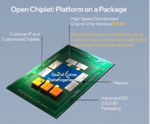
Upon incorporation of the new UCIe industry organization later this year, member companies will begin work on the next generation of UCIe technology, including defining the chiplet form factor, management, enhanced security, and other essential protocols (Figure 1).
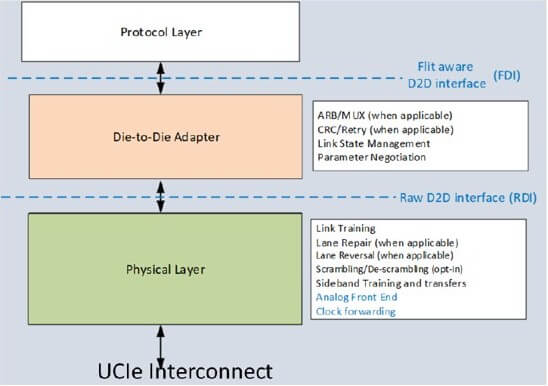
UCIe is a layered protocol, as shown in Figure 2. The physical layer is responsible for the electrical signaling, clocking, link training, sideband, etc. The die-to-die adapter provides the link-state management and parameter negotiation for the chiplets. When multiple protocols are supported, it defines the underlying arbitration mechanism.

UCIe maps PCIe and CXL protocols that are widely used at the board level across all segments. With PCIe and CXL, SoC construction, link management, and security solutions that are already deployed can be leveraged to UCIe. The usage models addressed are also comprehensive including data transfer using direct memory access, software discovery, error handling, etc., The memory use cases are handled through CXL.Mem; and caching requirements for applications such as accelerators are addressed with CXL.cache. UCIe also defines a “streaming protocol” which can be used to map any other protocol.
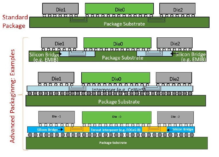
UCIe 1.0 defines both standard 2D packages and advanced packaging such as those using interposers and bridges (Figure 3). The UCIe specification reportedly encompasses all types of packaging choices in these categories.
UCIe supports two broad usage models. The first is package-level integration to deliver power-efficient and cost-effective performance from components attached at the board level such as memory, accelerators, networking devices, modem, etc. The second usage is to provide off-package connectivity using a different type of media (e.g., optical, electrical cable, mmWave) using UCIe to transport the underlying protocols (e.g., PCIe, CXL) at the rack.
In the future, the consortium expects to drive more power-efficient and cost-effective solutions as bump pitches continue to shrink and 3D integration becomes mainstream. Those may require wider links running slower and get closer to on-die connectivity from a latency, bandwidth, and power-efficiency point of view.
For all the latest in advanced packaging stay linked to IFTLE………………….


