
Will TSMC build advanced packaging facilities offshore?
In IFTLE 490, we reported that TSMC is considering building an advanced IC packaging plant in the US.
Now, from the Asia Times we learn in an article by Scott Foster, an analyst with Lightstream Research – Tokyo that in February, it was reported in both Japan and Taiwan that TSMC was planning to establish an R&D center in Tsukuba Japan to develop 3D IC packaging materials in cooperation with its Japanese suppliers.
In May, Japan’s Ministry of Economy, Trade, and Industry (METI) announced that more than 20 Japanese companies would be working with TSMC Japan’s 3D IC R&D Center. While METI’s announcement made headlines in Japan and Taiwan, I have not seen it discussed in the US.
The list of materials-making companies involved includes Asahi Kasei, Ibiden, JSR, Shin-Etsu Chemical, Shinko Electric Industries, Sumitomo Chemical, Sekisui Chemical, Tokyo Ohka, Nagase & Co., Nitto Denko, Nippon Electric Glass, Fujifilm, Showa Denko Materials (formerly Hitachi Chemical) and Mitsui Chemical. The list of equipment-makers includes Keyence, Shibaura Mechatronics, Shimadzu, Showa Denko, Disco, Toray, Nitto Denko, and Hitachi High-Tech. Also included are Fujifilm, Panasonic, Ajinomoto, Uyemura, Ebara, Shinkawa, Dai Nippon Printing, Disco, Tokyo Ohka, Namics, and Yamaha Robotics.
All of these companies are industry leaders with significant market shares in products crucial to the semiconductor industry. While they do have some competition in the US and Europe, their market position is the result of decades of manufacturing experience, a highly competent workforce and long-term relationships developed with customers. It is not an exaggeration to say that Japan has the most comprehensive assembly and packaging supply chain in the world.
TSMC Chip Facility in Japan
Focus Taiwan reports that TSMC is reportedly finalizing a decision to establish its first chip factory in Japan, which could start operations as early as 2023.
The planned factory on the southern island of Kyushu would produce around 40,000 28nm chips per month. It would mainly be used to supply Sony Corp., TSMC’s biggest client in the country, the report said. The Kumamoto factory would mainly be used to produce image sensors for Sony, which are used in devices such as digital cameras.
According to the report, TSMC’s final decision could be swayed by factors such as Japanese government incentives commitments by Japanese suppliers to build the chip-related infrastructure necessary for the development of supply chains.
More on US Onshoring
In June of 2021, The US Government issued a report entitled “Building Resilient Supply Chains, Revitalizing American Manufacturing, and Fostering Broad-based Growth”, which included reviews by the Departments of Commerce (semiconductor manufacturing and advanced Packaging), Defense (minerals and materials), Energy (large capacity batteries) and Health & Human Services (pharmaceuticals) of the status of these industries in the US.
The report, “Semiconductor Manufacturing and Advanced Packaging” notes that “semiconductors are an essential component of electronic devices. The packaging, which may contain one or more semiconductors, provides an alternative avenue for innovation in the density and size of products. Semiconductors have become ubiquitous in today’s world. They enable telecommunications and grid infrastructure, run critical business and government systems, and are prevalent across a vast array of products from fridges to fighter jets…The U.S. share of global semiconductor production has dropped from 37% in 1990 to 12% today, and is projected to decline further without a comprehensive U.S. strategy to support the industry…U.S. companies, including major fabless semiconductor companies, depend on foreign sources for semiconductors, especially in Asia, creating a supply chain risk. Many of the materials, tools, and equipment used in the manufacture of semiconductors are available from limited sources, semiconductor manufacturing is geographically concentrated, and the production of leading-edge semiconductors requires multi-billion-dollar investments.”
The report continues that “…In addition to the central role they play in the U.S. economy, semiconductors are essential to national security. Semiconductors enable the development and fielding of advanced weapons systems and control the operation of the nation’s critical infrastructure. They are fundamental to the operation of virtually every military system, including communications and navigations systems and complex weapons systems…”
This report examines the semiconductor supply chain through five segments, (1) design; (2) fabrication; (3) assembly, test, and advanced packaging (ATP); (4) materials; and (5) manufacturing equipment, which they summarize as follows:
Design: The U.S. semiconductor design ecosystem is robust and world-leading. U.S. design companies depend on limited sources of intellectual property (IP), labor, and manufacturing that are essential to bringing products to market.

Fabrication: The United States lacks sufficient capacity to produce semiconductors. The United States relies primarily on Taiwan for leading-edge logic chips and relies on Taiwan, South Korea, and China to meet the demand for mature node chips.
Advanced Packaging: For relatively low-tech back-end semiconductor ATP, the United States is heavily reliant on foreign sources concentrated in Asia. Furthermore, as chips become increasingly complex, advanced packaging methods represent a potential area for significant technological advances. However, the United States lacks the necessary materials ecosystem and is also not a cost-effective location to develop a robust advanced packaging sector.
Materials: The production of semiconductors requires hundreds of materials, presenting challenges in manufacturing supply chains. Many of the gases and wet chemicals for semiconductors are produced in the United States, but foreign suppliers dominate the market for silicon wafers, photomasks, and photoresists.
Manufacturing Equipment: The United States has a significant share of global production of most types of front-end semiconductor manufacturing equipment, with the notable exception of lithography equipment production, which is concentrated in the Netherlands and Japan. With limited semiconductor manufacturing occurring in the United States, these equipment manufacturers are heavily reliant on sales outside of the United States.
Their summary of “ATP” follows:
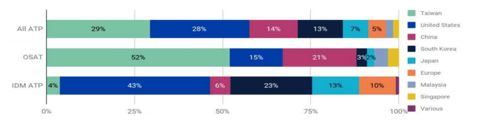
“In the back-end – or assembly test and packaging (ATP) stage, chips are assembled into finished semiconductor components, tested, and packaged for incorporation into finished products. The ATP stage occurs under two models: (1) by IDMs and foundries or (2) by Outsourced Semiconductor Assembly and Test (OSAT) companies that specialize at the test and assembly business and provide services on contract. While U.S. companies have 28 percent of the market share of ATP revenues and 43 percent of the market share of IDM ATP revenues … companies have outsourced ATP production to facilities outside the United States. Foundries such as TSMC (Taiwan), UMC (Taiwan), SMIC (China), and XMC (China) have entered the packaging business to increase the manufacturing services they offer to their fabless customers, especially the advanced packaging of chiplets. TSMC introduced its first advanced packaging solution in 2012. Market shares by region are shown in Figure 1.
They continue “While… ATP has historically been a low-value component of the supply chain, the packaging is increasingly becoming more advanced. For decades, the semiconductor industry has followed Moore’s Law, which provides that the number of transistors on a semiconductor doubles roughly every two years. Today, the power and performance benefits of chip scaling are diminishing at each new node while the cost per transistor has been increasing. While scaling remains an option, as it becomes more expensive and difficult, the semiconductor industry is searching for alternatives, including putting chiplets and/or more than one integrated circuit into one package. This is known as advanced packaging.
Advanced packaging represents both an alternative and complementary technology to linewidth shrinks as it offers higher chip density at the packaging instead of the chip level and allows for the integration of different chip functions in a single package. Advanced packaging also allows for increased use of commercial-off-the-shelf (defense-approved) chips for custom solutions. Advanced packaging types include chip stacking technologies—especially for memory chips— and embedded die, fan-out wafer-level packaging, and system-in-package (combining chiplets or multiple chips in one package).
One approach with logic chips has been to separate standardized IP functions into distinct, smaller chips, called “chiplets” that are connected via standard interfaces on a single package. A chiplet functions with other chiplets, so the design must be co-optimized and the silicon cannot be designed in isolation. The Defense Advanced Research Projects Agency (DARPA) and the Department of the Navy as well as industry participants … have had a number of projects exploring this approach. Advanced packaging has significant value for national security to enable disaggregation … thus allowing customizable devices for unique national security applications.
Recommendations include:
- Provide dedicated funding for semiconductor manufacturing and R&D: We recommend that Congress support at least $50 billion in investments to advance domestic manufacturing of leading-edge semiconductors; expand capacity in mature node and memory production to support critical manufacturing, industrial, and defense applications; and promote R&D to ensure the next generation of semiconductors in developed and produced in the United States.
- Establish a new Supply Chain Resilience Program: We recommend that Congress enact the proposed Supply Chain Resilience Program at the Department of Commerce, to monitor, analyze, and forecast supply chain vulnerabilities and partner with industry, labor, and other stakeholders to strengthen resilience. We recommend Congress back this program with $50 billion in funding that will give the federal government the tools necessary to make transformative investments in strengthening U.S. supply chains across a range of critical products
- Deploy the Defense Production Act (DPA) to expand production capacity in critical industries: We recommend establishing a new interagency DPA Action Group to recommend ways to leverage the authorities of the DPA to strengthen supply chain resilience to the extent permitted by law. The DPA has been a powerful tool to expand the production of supplies needed to combat the COVID-19 pandemic and has been used for years to strengthen Department of Defense supply chains. The DPA has the potential to support investment in other critical sectors and enable industry and government to collaborate more effectively.
For all the latest in Advanced Packaging stay linked to IFTLE……………………


