
Let’s take a final look at some of the presentations from the 2021 IMAPS Device Packaging workshop.
Applied Materials
Applied Materials (AMAT) discussed “Through Silicon Vias (TSVs) and Hybrid Bonding Solutions for Heterogeneous Integration…”. AMAT notes that hybrid bonding is not a new technology but rather has been commercialized for many years in CMOS Image sensors (CIS). Readers of IFTE have been following this technology since the early 2000s when Ziptronix was introducing it to the CIS community. It is also commercialized in YMTC NAND stacking.
In Figure 1, AMAT projected the following die stacking trends for DRAM with TSVs in 16 die-stacking being 3µm in die and 30µm high. They predict these will be done using copper hybrid bonding.

The new generations of DRAM using hybrid bonding for stacking will require lower temperature processes (<250°C) to avoid memory degradation issues. AMAT offers low-temperature chemical vapor deposition (CVD) oxide deposition tools and lower-temperature Cu-Cu bonding solutions by depositing specific Cu orientations that have much higher surface copper diffusivity.
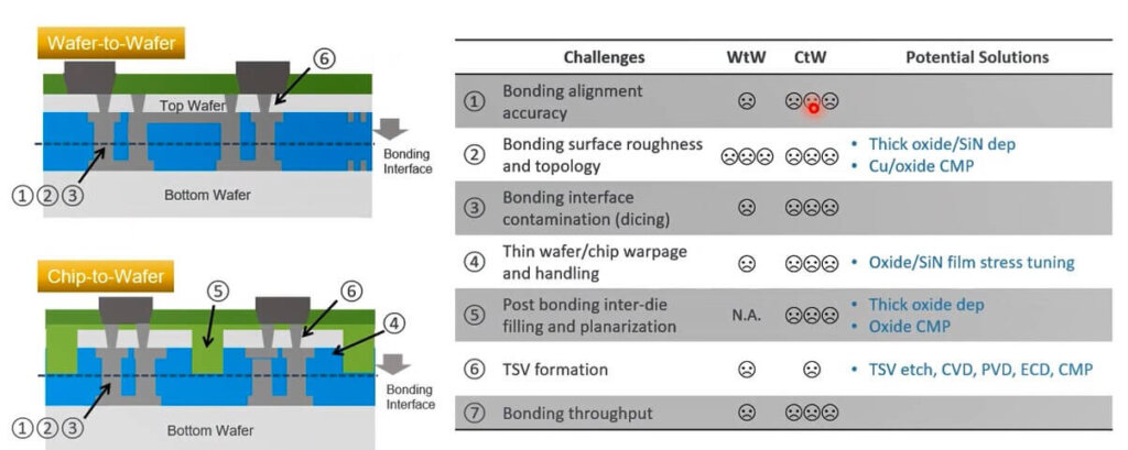
In Figure 2, AMAT notes integration challenges for W2W and C2W hybrid bonding, noting that chip-to-wafer is “more complicated and harder”.
AMAT is working with BESI to offer a complete toolset for hybrid bonding. They have set up a center of excellence in Singapore.
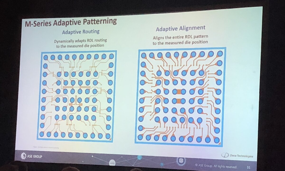
DECA M-Series
For those of you that always wanted to better understand the adaptive patterning technology used for the M-Series fan-out packaging developed by DECA and being scaled by ASE and Nepes, Craig Bishop gives a super detailed presentation on exactly how this is done. If you’re interested in the details, IFTLE highly recommends this presentation. We are talking here mainly about die displacement upon over-molding, both X and Y shift, and rotation, which can have an even bigger impact on larger die. After die placement, they basically map the positions of all these die from which the RDL via pattern is adaptively aligned to the exact die position and adaptive routing that adjusts the RDL routing between die.
Figure 3 shows a cross-section of the M-Series fan-out structure.

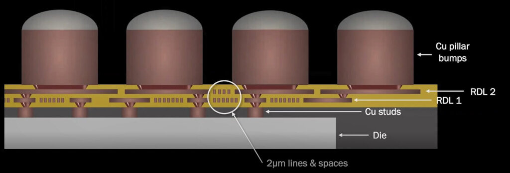
Basically, they transfer any die miss alignment (die shift) away from the fine pitch upper stud interface on the die up to the much larger pitch interface of the copper pillar bumps.
If the die shift is large compared to the bump pitch, you may still get shorting. To resolve this, they have developed “progressive adaptive alignment” where the die shift is distributed across multiple layers of the RDL so the top layer doesn’t have to handle it all.
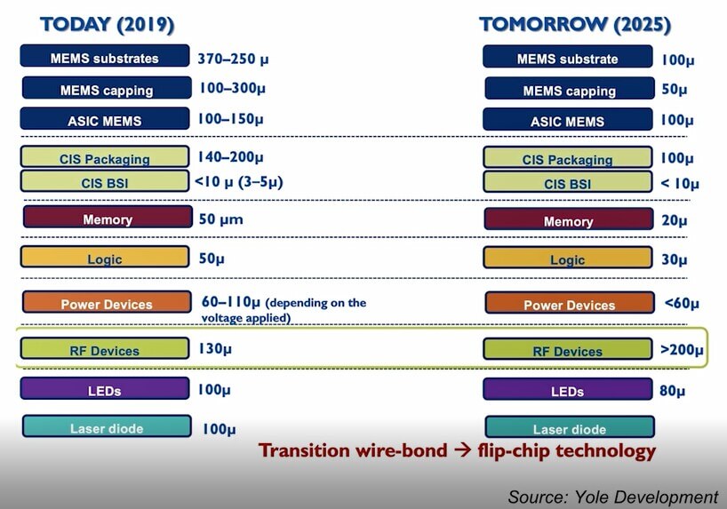
Corning
In their presentation on “Glass Carriers with Matched CTEs for Wafer Thinning Applications,” Corning shows us a Yole Développement projection on the expected thinning for various devices in 2025.
For all the latest on Advanced Packaging stay linked to IFTLE……………………….


