
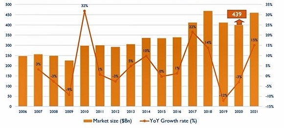
Vaibhav Trivedi of Yole Développement gave an outlook for the advanced packaging market with a focus on 3DIC. The semiconductor market declined 12% YoY to reach $412B in 2019. In 2020 the market grew slightly despite the pandemic to about $439B. Yole expects 2021 to be another slight growth year (Figure 1).
Smartphone and tablet demand is expected to stay flat over the next 5 years with ~ 1.3% growth while wearable devices (watches, earbuds) are expected to grow 14%.
In 2014 advanced packaging accounted for 38% of the total packaging market. Its market share is expected to increase to ~49% ($43B) by 2025.
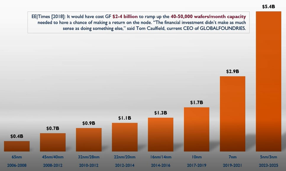
As we have discussed in IFTLE numerous times, scaling for the majority of IC fabricators has ended. The only players left moving past 10nm are TSMC, Samsung, and Intel, and as we have discussed Intel appears stuck at 10nm due to yield issues. The cost of a 5nm fab is expected to be in the range of $5B as shown in Figure 2.
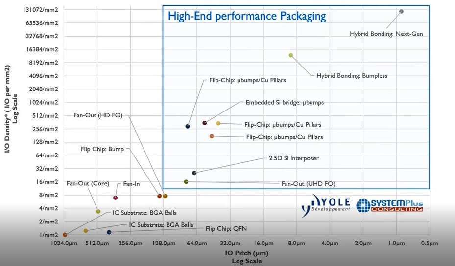
Yole defines high-end packaging as state-of-the-art packaging that value-adds device performance with high I/O density (>16/mm sq) and tight I/O pitch (< 130µm). Typical technologies are shown in Figure 3.
3D packaging provides another lever that can be used without scaling the front-end silicon while providing higher performance and bandwidth compared to traditional packaging.
A look at high-end performance 2.5/3D packaging segmentation is shown in Figure 4:
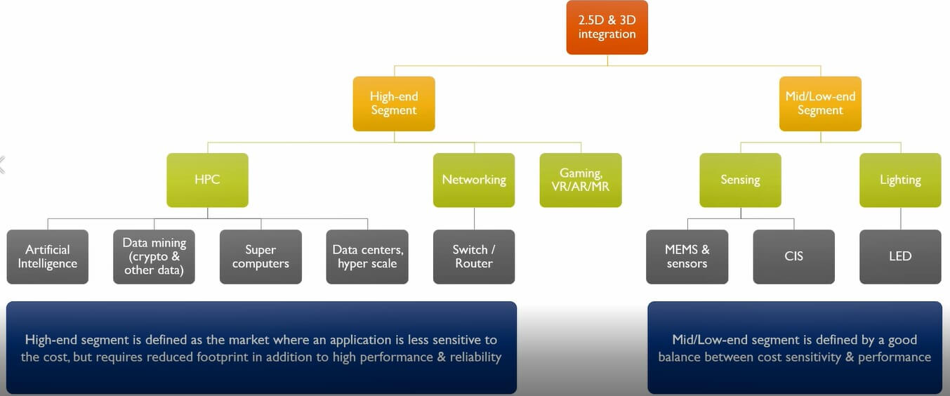
Mid to low-end packaging focuses on sensors and lighting while the high end focuses on high-performance computing and networking solutions. Yole projects the 3D packaging unit forecast going from 3.3B units in 2020 to 7.8B units in 2026 with revenue going from $1.6B in 2020 to 6.7B in 2026.
They expect 3D packaging to accelerate the growth of heterogeneous integration. As IFTLE readers already know, Intel, TSMC, and Samsung, traditional IC leaders are now the leaders in high-end 3D packaging options.
In 2020 Samsung announced the availability of its 3D X-cube technology. X-cube is built with 7nm technology using through-silicon vias (TSVs) to stack SRAM on top of logic as shown in Figure 5.
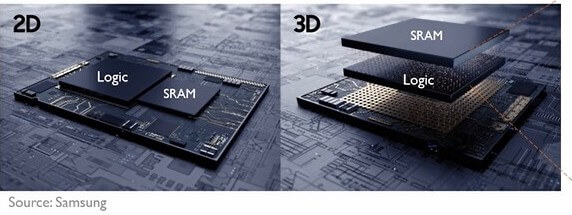
Figure 5: Typical 2D side-by-side package vs. 3D IC stacked package. ((Courtesy of Yole Développement)
3D stacking products are now widely being used as can be seen in Figure 6.

TSMC is investing heavily in its advanced packaging infrastructure. Intel is using packaging to bridge the gap as it delays the launch of 7nm to 2022 or beyond. OSATS and EMS providers are contributing to advances in heterogeneous integration through their SiP product lines (i.e modules, MCMs).
For all the latest in Advanced Packaging stay linked to IFTLE…………………………….