

I think it was Shakespeare who reportedly penned, “Would a rose by any other name still smell as sweet?” or something close to that. Why am I quoting Shakespeare? Well, we have a technology, massively parrallel pick-and-place assembly, that’s been around for more than a decade that I think still suffers by being originally miss named, but that should not stop us from using it in applications where it is applicable.
You may also be saying “why are we about to discuss a technology that’s been around 15 years and hasn’t caught on commercially yet?” Well, let me stop you right there. You’re probably the same folks that questioned why I kept reporting on Ziptronix and its Direct Bond Interconnect (DBI™) technology. That also took more than a decade to catch on, but now, acquired by Xperi and known widely as hybrid bonding, it is on the roadmaps of all major packaging players like Intel and TSMC. That’s Why…
The Massively Parallel Pick-and-Place Back Story
This will take just a bit of historical introduction so bear with me.
Fifteen years ago (2006), about a year or so after I had left Dow Chemical to start my own consulting company, I was approached by longtime friend, Joe Carr, with whom I had worked for many years at Dow. He had also moved down to North Carolina and was about to become CEO of a spinout of John Rogers’ (University of Illinois). Rogers and his students had developed an assembly technology using polydimethylsiloxane (PDMS) stamps to move very small, very thin chips and /or other devices and was looking to start a company to commercialize the technology. Carr had accepted the challenge and was looking for someone to help him staff up and find the right commercial applications. Since I wasn’t busy at the time, I agreed to help out part-time while building up Microelectronics Consultants of NC.
When Carr explained the technology to me, he said something like “Rogers calls it micro-transfer printing” In my usual sarcastic manner I answered back “Printing? this is pick-and-place technology” and Carr replied, “Yes, massively parallel pick-and-place technology.” So, from the beginning, we both knew exactly what it was. Why then was the technology called micro-transfer printing? Just guessing here, but maybe Professor Rogers felt “pick-and-place” wasn’t a fancy enough buzzword to get his academic articles into “Nature” or one of those journals that consider themselves above all the rest.
Anyway, the company was named “Semprius” and a few years later, after we had staffed up, Semprius decided to focus on concentrated photovoltaic (CPV) panel fabrication. Recall back then anyone focused on solar got an abundance of government research dollars (think Solyndra). I was not the least bit interested in producing expensive energy, which all photovoltaics were and still are, so I left. Semprius succeeded, with state and federal government support, to put a factory in place in NC for solar panel manufacturing, but like the rest of these solar activities couldn’t compete with cheaper Chinese panels in the market and eventually folded.
While Semprius was focusing on solar panels, X-Celeprint was formed when X-Fab’s parent, Melexis, bought the rights to all non-solar applications for micro-transfer printing from Semprius. Having developed some interesting technology for microLED display manufacturing, X-Display, under Chris Bower, spun off a few years later to manufacture microLED displays leaving X-Celeprint with all non-solar panel, non-display applications.
AKA: Micro Transfer Printing Technology
So that’s where we are today. It’s been over 15 years since the first PDMS stamp picked up the first sliver of silicon so I thought it might be useful to look at what the X-Celeprint MTP group … Let’s call them “the X-Men” … have developed over this period. It just might be the assembly technology you’re looking for.
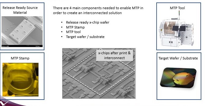
X-Celeprint is basically a licensing company for micro-transfer printing (MTP) technology. It is headquartered in Cork Ireland with a US development site in Research Triangle Park NC. A one-slide description of MTP is shown in Figures 1 and 2, followed by a look at what is needed to practice MTP.
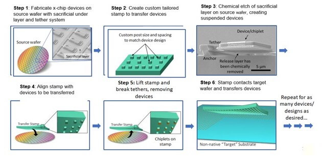
The Source Wafer
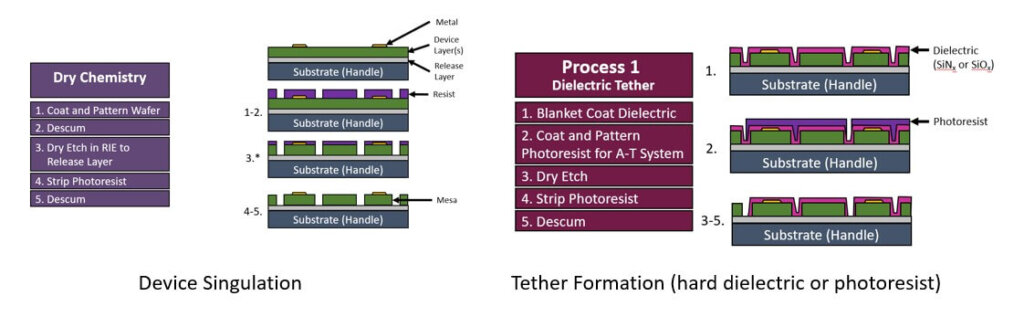
Source wafer fabrication is shown in Figure 3. Demonstrated source materials include semiconductor materials such as silicon CMOS (SOI), InP, GaAs and GaN.
X-Celeprint has partnered with X-Fab to develop an XT018 SOI print-ready process. The company is working with other partners to develop similar SOI and III-V capabilities. They offer services in both North Carolina and Cork, Ireland to create print-ready source wafers for prototyping. X-Celeprint calls chips that have been fabricated to be used in MTP “X-chips”.
The Stamp
A stamp master is fabricated in silicon with standard fab photo processes. PDMS is then cast between the stamp master and a sheet of glass in a glass mold (Figure 4). The assembly is then cured, and the glass and PDMS are separated from the stamp master. The spacing of the PDMS “nubs” are set based on the pitch of the chips desired for removal from the source wafer.
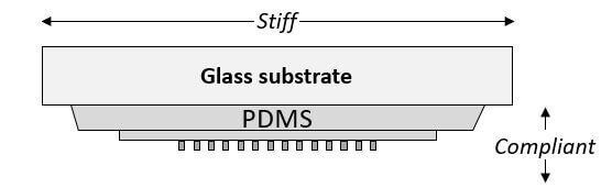
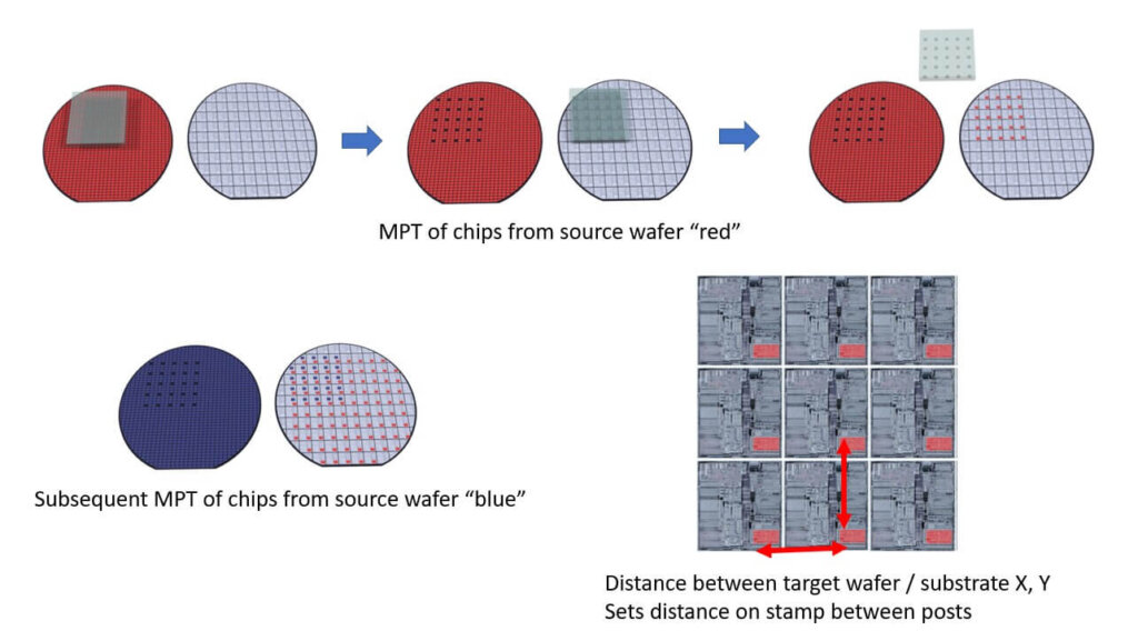
Figure 5 shows an example of the pick-and-place of “red” and “blue” chips to a packaging substrate, interposer or chip-on-chip stacking. MTP allows for densely packed devices to be fabricated on its’ native substrate. A custom stamp is created that will match the pitch of the receiving substrate in X and Y dimensions.
The MTP Tool for Massively Parallel Pick-and-Place Technology
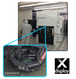
Currently, there are two companies producing MTP tools, X Display Corporation and ASM/Amicra (Figure 6). The tools are 200 -300mm capable. Gen 4.5 panel tools being planned.
Target Substrate
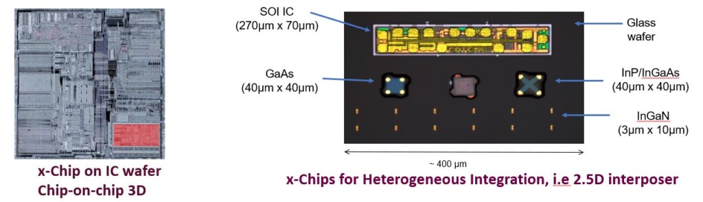
Target substrate selection is dependent on the application. MTP target substrates can be a variety of materials (Si, glass, plastic, ceramic). As shown in Figure 7, X-chips can be moved to 2.5D interposers for heterogeneous integration or onto silicon wafer devices for chip-on-chip bonding.

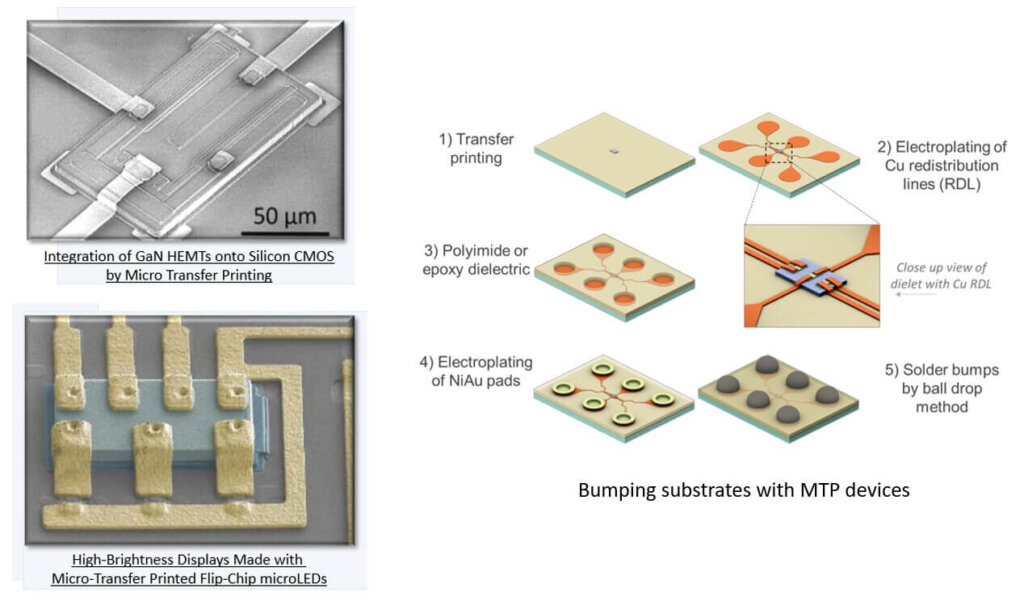
For these chip-on-substrate or chip-on-chip applications, the connection is made by the fabrication of simple thin-film copper (or I would think just as easily gold) interconnect. MTP printed devices can reportedly be connected and bumped with standard semiconductor processing as shown in Figure 8.
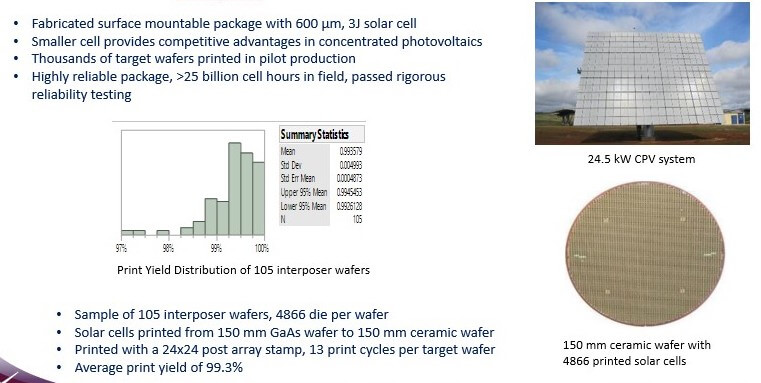
Yield has been best studied for the commercial solar panel application. As shown in Figure 9, for the conditions shown, the print yield was 99.3%.
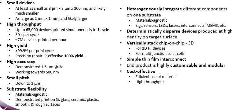
Print accuracy was extensively studied while developing the micro-LED display application. Transfer of 690K display drivers resulted in a mean print yield of 99.6% and a print accuracy of +/- 1.5um (3 sigma).
Repair of the printing can be achieved post-printing of the target substrate in multiple ways using a single post stamp to pick and print single chips depending on the final yield need. A summary of MTP attributes is shown in Figure 10.
Keep this technology in mind if you are looking for any of these assembly requirements.
Download this summary presentation ton MTP to learn more.
For all the latest in advanced packaging stay linked to IFTLE……………………


