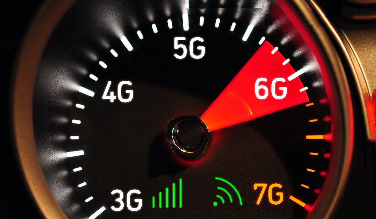
iNEMI recently presented a webinar by Prof. Madhavan Swaminathan who has taken over Georgia Tech’s Packaging Research Center, after Rao Tummala’s retirement. The topic of advanced packaging for 5G and the upcoming 6G is certainly of interest to all so let’s take a closer look.
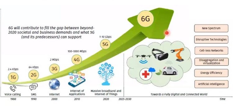
While 5G is expected to max out at ~20Gbps, 6G should take us to 1Tbps. Current 5G offers connectivity of ~ 106devices / km2 (Figure 1).
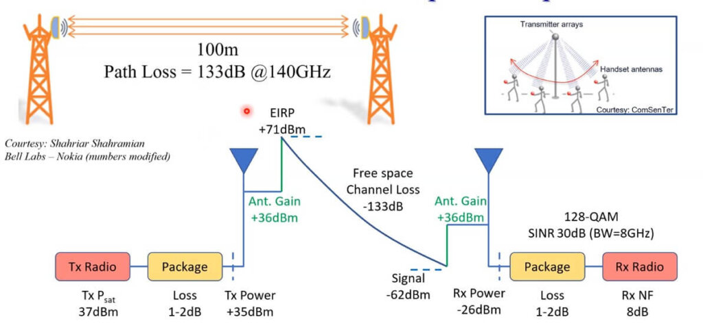
An example of the losses incurred sending signals between cell towers that are currently spaced 100meters apart, as shown in Figure 2.
As we continue to increase frequency, signal losses increase and must be compensated for. Rf packaging becomes the key enabler. Advanced packaging will be needed for:
- Reduced signal losses / higher antenna gain
- Heterogeneous integration for mixed semiconductor solutions
- Thermal management
Antenna-in-package will become a necessary technology to bump up signal power. As you go up in frequency you need more and more antenna elements to obtain the required signal “gain”.
Ga Tech believes glass will be the key material for the Rf packaging needed for these solutions.
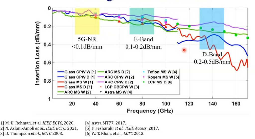
The figure below shows expected losses vs 5G, E band, and D band frequencies (Figure 3).
It is expected that these packages will be built in 3D as shown in Figure 4, with beamformers, power amps, and antenna patches in the stack with electronics beneath the antenna to reduce form factor and loss. They will be built with polymer dielectric dry films that have low Dk and Df.

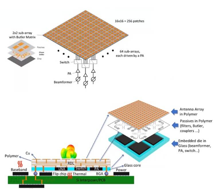
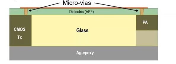
Chip embedding in the glass interposers will be important since the required heterogeneous integration ( CMOS chips and InP PA chips) deals with chips of different thicknesses and need to be compensated for by the pockets holding them in the glass. Connections will be made directly by microvias eliminating the loss from flip-chip bumps which in turn are 10X less lossy than wire bonds. Ag/epoxy is used to pull heat out the bottom of the interposer. The micro vias are low-loss solutions (typically 0.15dB / mm).
Swaminathan concluded that wireless integration was only part of the puzzle and it would have to be combined with photonics and sensing to give us a complete solution.
For all the latest on Advanced Packaging stay linked to IFTLE………………………………….