
Introduction
Product burn-in (BI) is an indispensable step in the production test flow to ensure good quality and a properly functioning product for the customer. Amkor takes pride in rating ‘quality delivered to the customer’ as one of the highest corporate virtues. See Figure 1.
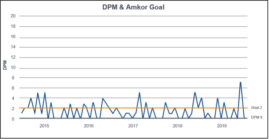
Burned-in integrated circuits (ICs) have a much lower failure rate during their operating life than ICs which are not burned-in. As a result, test services with burn-in test equipment should be available as a customer option.
The Reliability Bathtub Curve and the Impact of Burn-in Test
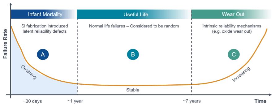
Researchers have shown that the reliability failure rate starts off high, as shown in Phase A in Figure 2, then eventually drops to a constant level, as shown in Phase B. Manufacturers use burn-in to remove the devices that make up early life failures before the product is shipped to the customers. Early life “infant mortality” failures are trapped by subjecting the IC to accelerated life test conditions, including elevated voltages and temperatures. Even with the early failures removed from the population, the failure rate is reduced but never eliminated [1]. No amount of product burn-in completely eliminates all failures. The failures in the useful product life (Phase B) are random in nature and cannot be traced back to be a systemic fabrication or design-related failure.
An increase in the failure rate is again observed toward the end of the useful life. This increase in the failure rate (Phase C in Figure 2) is attributed to effects like oxide wear out, electromigration, time-dependent dielectric breakdown and others [2].
Latent defects are screened by application of stress (burn-in) conditions that accelerate the cause of defects. Below is the Arrhenius equation for reliability that is used to calculate a thermal acceleration factor for a given observed time-to-failure:
AT=e^[(-Eaa/k)(1/T1 -1/T2)]
Equation 1
In this equation, AT is the acceleration factor due to changes in temperature, Eaa is the activation energy (eV), k is the Boltzmann’s constant (8.62 x 10⁻⁵ eV/K), T1 is the absolute test temperature (K) and T2 is the absolute system temperature (K). This equation helps the quality and reliability engineering team to compute and model-specific burn-in conditions for specific silicon fabrication technologies, product designs and infant mortality (IM) goals in terms of burn-in voltage, burn-in temperature and burn-in time. Burn-in voltage is typically about 30% higher than the application use voltage and the burn-in temperature is typically between 95°C to 105°C. These values result in a burn-in time (BIT) that could be a couple of seconds to a couple of minutes and, depending on the die size, a couple of hours.
Burn-in is typically the first test step in the test flow after assembling the probed and sawed wafer die into packages. While burn-in of packaged parts is popular with a large fraction of customer devices, wafer-level burn-in may become important to the fraction of the product volume targeted for mobile and handheld end applications in the future.
The benefits of burn-in concepts apply similarly for almost all fabrication technologies of digital, analog and radio frequency (RF) ICs. Some Integrated Device Manufacturers (IDMs) request burn-in test services for ICs that have digital logic, analog and RF end applications targeted for automotive, industrial and commercial use. Memory product’s burn-in test methodology focuses on retention of data in addition to the logic test methodologies for combinational logic products. IC designers architect the test content (patterns) to ensure maximum toggle coverage. Boundary-scan, structural-based functional test (SBFT) and built-in self-test (BIST) test patterns require limited product tester resources (signals and clocks). However, due to elevated voltage requirements, the power supply and power delivery path of each device voltage rail are critical.
It is worth noting that some of the mature process technologies for which the infant mortality and failure signatures are well understood or have been removed with process optimization may benefit from sample burn-in monitoring and complete elimination of burn-in from the production test process flow. Packages with multiple die that employ different process technologies and logic types, require complex burn-in test flows to ensure that quality objectives are met.
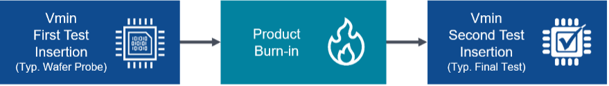
The impact of the burn-in stress is measured in terms of Vmin degradation between wafer sort and final test of the same device as shown in Figure 3.
Burn-in Test Equipment
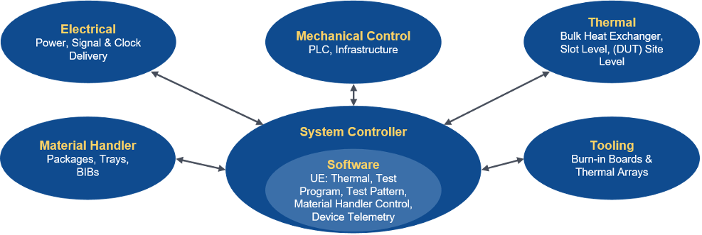
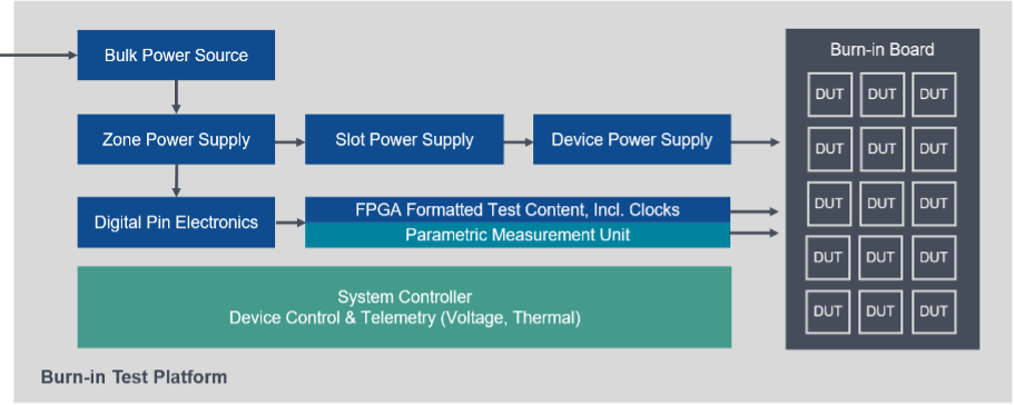
Burn-in test equipment has a handful of key functional blocks that are vital to dispense an effective burn-in environment to the devices under test (DUTs). Due to traditionally limited test content relative to Final Test, the test equipment by design caters to a massively parallel device test platform. A typical test platform has one to six zones. Each zone has a provision of 12 to 18 slots and each slot is capable to burn in eight to a couple of hundred units concurrently. While this document discusses platforms that include automated DUT and burn-in board (BIB) handling, there are burn-in platforms that do not have these capabilities automated. In such cases, the loading and unloading of DUTs and BIBs are performed manually. The parallelism and asynchronous handling of zones, slots with a zone and slots themselves depend on the end application (memory or logic, package constraints, thermal constraints and more) and the supplier’s equipment definition for the custom application market.
Software Sub-System:
The Burn-in test platform is controlled with a system controller, where software controls individual sub-blocks of the platform. The test controller runs proprietary tester operating system (TOS) software that controls all functions of the system with a test program or test recipe that subjects the DUTs with burn-in tests under stressed conditions. The handler recipe may be able to command the DUTs in a JEDEC tray to be loaded (or unloaded) into the BIBs and then load (or unload) the BIBs into specified slots within a zone. The test program contains software commands that instruct the electrical hardware to turn on (or off) the device power supply rails in a specified sequence to apply the burn-in voltage to the DUTs, heat up the DUTs to the burn-in temperature or execute test patterns that test the parts and generate heat to achieve the desired burn-in temperature.
Electrical Sub-System:
Facilities AC power that is fed to the electrical sub-system is conditioned with a bulk power supply that feeds AC or DC power to all components within the burn-in platform. There is a large range of steady-state and transient power requirements for each product. There are products in every power range from 10’s of watts to 100’s of watts. DUT clocking and data (signal) requirements, within the test pattern executed, vary based on the end-product application. DC power delivered to each of the zones and each slot within the zones drive the isolated voltage regulators that output filtered DC rails up to 2 to 3 rails per DUT. Voltage regulator outputs are programmable with a voltage range between 0V and 8V for DUT power and up to 24V for heater power. Typical DUT voltage signal swings are 1.2V, 1.5V, 2.5, 3.3V or 5.0V. Device power force and measurement accuracy for burn-in may not be as challenging as Final Test, however, they are still are <±20 mV and the resolution is <±2 mV. Device clocking requirements are <200 MHz. A tester clock must have low total jitter, typically <100 pS, to be able to effectively drive the phase-locked loops (PLLs) on-board the device. Clock distribution to all DUTs is important to the BI application.
Traditional processors have an IEEE 1149.1 Joint Test Action Group (JTAG) compliant Test Access Port (TAP) [4] to send and receive boundary scan and BIST content along with a handful of static control digital pins. The TAP is a relatively simple five-pin serial interface with a finite state machine [4] that provides Design for Excellence (DFX) needs for all devices for over decades. Traditional wide I/O memory BI requires a memory controller, test-mode dependent number of I/O pins. The number of I/O pins per DUT, in this case, may be as high as 128 to 150 pins. The typical signal interface for BI is limited to less than about 200 Mbps. Over the past decade, there has been pressure to utilize the massively parallel BI topology’s cost-effectiveness and re-locate Final Test content to the burn-in test step. However, the trade-offs between content and test equipment complexity and cost must be considered.
Thermal Sub-System:
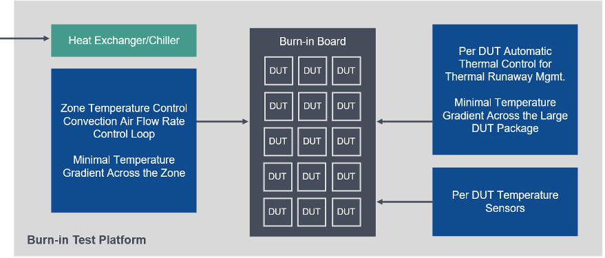
A tight Isothermal device environment is vital to ensure the devices are subjected to the appropriate and consistent magnitude of burn-in. Integrated circuits heat up as power is applied to them. They generate additional heat as clocks are applied and various parts of the device logic and analog/RF blocks are exercised. Depending on the size and design of the package, the thermal mass may be adequate to allow the device under test to reach burn-in temperatures, while in other smaller packages, additional BIB or socket heater power may be required to achieve the desired burn-in temperature. Burn-in equipment achieves a tight isothermal environment by providing device voltage rails with sufficient resolution and accuracy. Burn-in equipment is designed such that the chamber’s zone and individual DUT thermal arrays and heaters can effectively and quickly respond to dynamic changes in operation and package variations. Another important aspect unique to the burn-in test step is that this test step must deal with products from all process flows. With accelerated test conditions, ‘high leakage,’ shorted or thermal runaway parts are typical outliers. Higher power distribution parts may require, voltage rail folding to ensure they do not thermally ‘run-away.’ The burn-in equipment is designed to ensure safe factory operation by trapping all conditions that may result in catastrophic events.
Mechanical and Material Handling:
It is important for the critical mechanical dimensions of the burn-in test platform to be such that it fits well within the factory’s facility constraints. The platform’s footprint must utilize the factory floor space effectively for maximum throughput. The facility’s power and process chilled water (PCW) inlet and outlet can be adapted to local factory requirements. Regular maintenance of parts and thermal fluids for temperature range of operation can be easily sourced and cost-effective. The material handler, in some cases, is fully automated and handles product dispensed in trays.
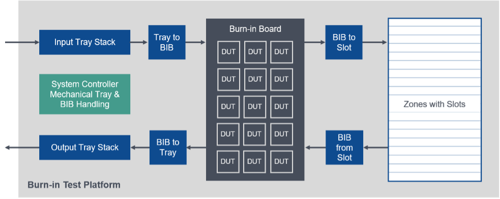
DUTs in trays are installed into sockets on the burn-in boards for production testing and then returned to stacks of defined hardware bins to the factory operator.
Tooling:
The burn-in platform is customized (tooled) for a product with custom burn-in sockets and thermal arrays that match the product’s package form factor. This means that while the remainder of the burn-in platform is device agnostic, the BIBs are not. The number of devices per BIB slot makes up for a complexity that is important to manage. Socket type, socket pin type and number of pins per socket for the package must be carefully selected to ensure cost targets are met. BIB printed circuit board (PCB) type selection is typically a FR4 variant, which is invariably acceptable in terms of cost and performance. The clock, signal, power and ground delivery path are carefully architected to ensure performance metrics are met.
Summary
Burn-in is a recognized important test step in the production test flow. As part of this process, advanced automated factory systems continuously monitor the quality and reliability metrics. Partnering with the best burn-in test equipment suppliers whose equipment not only meets test attributes but also has the maximum throughput, provides test customers best-in-class burn-in test services with maximum performance envelopes and at an economical price point.
References
- The Quality and Reliability Requirements – Internet Source.
- Calculating Useful Lifetimes of Embedded Processors – Internet Source.
- JEDEC – The Arrhenius Equation for Product Reliability – Internet Source.
- IEEE Standard Test Access Port and Boundary Scan Architecture,” in IEEE Std 1149.1-2001 , vol., no., pp.1-212, 23 July 2001, doi: 10.1109/IEEESTD.2001.92950 – Internet Source.
- High Temperature Burn-In Board with sockets for semiconductor devices for a KES GenPower System. Internet Source. KES Systems is one of the many suppliers of Burn-In Boards & Sockets.