
2020 proved to us that our world is wholly unpredictable. As the year began with optimism for a new decade and excitement for what the new decade might bring, the last thing expected was the arrival of COVID-19. Within a short time, the pandemic created unprecedented disruption while shattering lives across the globe. Everything changed, and nations, industries, businesses, and people sought to quickly mobilize and establish best practices to navigate through the challenging days and months that have ensued. A huge debt of gratitude is owed to healthcare and essential workers that have faced risk head-on and sacrificed so much, and who continue to do so while the COVID-19 threat continues to surge.
Accelerating the Digital Transformation
The last year also demonstrated the extent to which technology is being used to solve some of the world’s greatest challenges. With digital transformation already on the horizon, the global pandemic meant that our world leapfrogged years ahead and the timeline for work from home, distance learning, and telemedicine significantly sped up. The future became our current reality, as technology was used across the globe to maintain continuity and mitigate disruption.
According to the Consumer Technology Association, there are 14.2B connected things in use and that number is expected to grow to 55B by 2025. This is resulting in an explosion of data. Our connected lives generate 2.5 quintillion bytes of data daily, driving unprecedented demand for bleeding-edge digital networks, connectivity, storage, memory, edge to cloud computing, and so much more. Data has become the oil fueling innovation growth across society, from health to entertainment, from home to business.
2021 has seen the role of the semiconductor industry further thrown into the spotlight. Since the industry began, applications from mainframe to minicomputer to PCs to the mobile space have inspired innovation and growth. It is well known that Moore’s Law has driven the industry for decades, but in recent years, there has been a deceleration in terms of performance and economic benefit. The exponential cost of silicon scaling has created an inflection point for the industry, and that is driving the development of More-Than-Moore technologies to augment increased device and system performance.
A Brief History of Semiconductor Roadmaps
Heterogeneous Integration refers to the integration of separately manufactured components into a higher-level assembly system-in-package (SiP) that in the aggregate provides enhanced functionality and improved operational characteristics. It is now the key technology direction going forward, driving the pace of advancement for greater intelligence and connectivity, higher bandwidth and performance, and lower latency and power per function, all at a more manageable cost.
The semiconductor industry comprises highly specialized yet closely interdependent companies that must stay on top of technology and market application trends to keep developments on track. It has been that way since the industry began in the 1950s, but as it grew, it became imperative by the 1990s that measures had to be taken to ensure that global semiconductor companies were progressing in the same direction. Industry leaders bandied together and reached a consensus to work side by side to establish a technology roadmap.
In 1991, semiconductor companies in the United States, under the auspices of the Semiconductor Industry Association (SIA), first established the National Technology Roadmap for Semiconductors or NTRS. By 1998, roadmapping efforts had expanded when companies from Japan, Europe, Korea, and Taiwan joined the NTRS effort, and together with SIA, they formed the International Technology Roadmap for Semiconductors or ITRS. SIA brought ITRS to a close in 2015, and that is when the Heterogeneous Integration Roadmap, or HIR, was initiated.
Heterogeneous Integration Will Take Us Forward
Just as Moore’s law led the advancement of the global semiconductor industry over the past 55 years, heterogeneous integration is and will be the key technology direction going forward. It is positioned to initiate a new era of technological and scientific advances to continue and complement scaling into the future. Packaging – from device packaging to system packaging – will form the crucial vanguard to this enormous advance.
The Heterogeneous Integration Roadmap (HIR) is a roadmap to the future of electronics, that identifies technology requirements and potential solutions. The primary objective is to stimulate pre-competitive collaboration among industry, academia, and government to accelerate progress. HIR is designed to provide long term continuity and a broad technology base. It is organized with sponsorship by three IEEE Technical Societies (Electronics Packaging Society, Electron Devices Society, and Photonics Society ) together with SEMI and ASME Electronics and Photonics Packaging Division (EPPD). Technology takes a long time to develop and mature, and increasingly involves the collective knowledge from overlapping fields. It is therefore essential to set goals for the long-run and cover as many subjects and fields as possible, related to heterogeneous integration.
Towards that end, the HIR is organized into 22 technical working groups (TWGs) covering diverse fields in the electronics industry comprising numerous experts and scientists from different disciplines across the globe. Recognizing that technology advances will be driven by advances in system integration in response to market applications, the HIR identifies six market application areas that will shape the electronics industry. These include high-performance computing and data centers, mobile applications, Internet of Things, automotive electronics, aerospace and defense, medical healthcare, and wearables. TWGs are grouped into these six market applications, as well as five building blocks technologies, eight cross-cutting technologies, and three integration technologies. Overall, the HIR contains 23 chapters including the executive summary.
As the industry enters the digital transformation and exascale computing era, massive compute with frequent access to data is required for high-performance computing (HPC) applications. The increasing amount of data from all sectors is raising the issue of operational and storing cost of the data. The advent of artificial intelligence (AI) and machine learning (ML) requires large amounts of data to be processed and is driving an entirely new computing paradigm from edge computing to cloud to data centers.
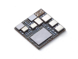
Traditional IC design trends are to pack more transistors on a monolithic die or system-on-chip (SoC) at each process node, resulting in difficult chip scaling for the integration of analog, logic, and memory circuits. The heterogeneous integration approach is die-partitioning or chiplets, which offers a compelling value proposition for yield improvement, IP reuse, performance, and cost optimization, as well as time-to-market reduction.

Chiplet integration has the potential to allow the integration of disparate technologies from multiple suppliers to provide more flexible mix-and-match systems to accelerate performance and improve power efficiency without requiring the deployment of these technologies across an entire SoC simultaneously. Chiplet solutions start with internal designs within a system integrator. However, as IP interface standards are developed, the commercialization of chiplets in the market will proliferate. Heterogeneous Integration through chiplets will play a critical role for future HPC and AI/ML applications.
As a leading semiconductor packaging, test, and system service provider, ASE has heavily invested in both chip-level (SoC) package integration and system-level integration. The development of cutting-edge heterogeneous integration technologies addresses functional areas from silicon integration, power integration, optical integration to system integration that form the backbone of many electronic components, subsystems, and electronics products.
ASE has developed and offers a wide portfolio of Si-level integration technology solutions, from low- to high-density chiplet integration including flip-chip multi-chip-module (FC-MCM), fanout chip-on-substrate (FOCoS), and 3D IC. The advanced FOCoS technology can provide short die-to-die connection and high interconnections (10,000s), redistribution layers (RDL) with 2µm line/space, and up to four layers for chip-first and chip-last packaging processes. It produces a lower-cost solution with improved electrical performance compared to a 2.5D Si interposer solution due to the elimination of Si through silicon via (TSV) processes and reduced insertion loss. ASE is evolving this advanced packaging platform to meet application demands for HPC and AI/ML applications.
A Smarter, Healthier, More Efficient Future
Semiconductor applications do exist everywhere in our daily lives today. Engineers constantly face significant challenges, albeit very different from the challenges faced by engineers in the 1960s. One cannot but be deeply motivated by a speech delivered by the former President of United States, John F. Kennedy on September 12, 1962, “We choose to go to the moon in this decade and do the other things, not because they are easy, but because they are hard because that goal will serve to organize and measure the best of our energies and skills, because that challenge is one that we are willing to accept, one we are unwilling to postpone, and one which we intend to win, and the others, too.”
Looking further into 2021 and beyond, key developments in packaging that create higher performance systems and utilize less power will be deployed. System performance will continue the pace of Moore’s Law era, albeit in a different way than with the previous total reliance on semiconductor chip lithography and SoC integration. There is tremendous optimism that innovations in the IC packaging industry will continue on a heterogeneous integration journey. Discovery, creativity, innovation, and very importantly, collaboration – will enable applications that make our world smarter, healthier, and more efficient. It is our hope to leave it in an infinitely far better place for future generations to live, work, play, and communicate.