The annual IEEE Electronics Packaging Technology Conference (EPTC 2020 – Asia’s equivalent to the ECTC) took place virtually in December, instead of in Singapore as originally planned. With most of the world’s packaging being done in Asia, it is always a great source of interesting advanced packaging presentations. Let’s take a closer look at what was presented this past fall.
Applied Materials – Automated Classification of RDL Defects
In a joint presentation between AMAT Bangalore and Singapore detailed Redistribution Layer Defect Classification Using Computer Vision Techniques and Machine Learning, they propose a solution involving computer vision techniques and Machine Learning (ML) to accomplish defect binning procedure is a typical wafer-level packaging scenario, focusing on 2µm L/S redistribution layer (RDL) feature sizes (Figure 1). They conclude that with this approach, inspection cycle time is reduced, thereby driving faster product development.
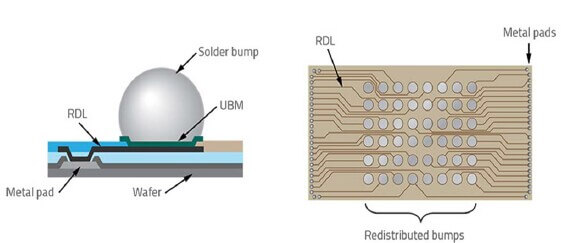
Inspection tools generate an RDL image within the wafer. These then need to be classified into various defects, namely: merged line, torn Line, bridged line, and particle. If no defect is found it is declared to be clean.
Computer vision techniques and ML were utilized to perform defect binning for 2/2µm L/S RDL features. A residual neural network was used as the first level classification between clean and defective images. The inspection cycle can be reduced significantly, from minutes to seconds.
Pixel-count algorithm, histogram-based intensity algorithm, and color-averaging algorithm were then employed to accurately classify different types of defect. They demonstrated over 90% accuracy of defect classification with this approach.
IME / Orbotech / Nordson Electronics – Through Mold Interconnect (TMI) Processing
IME, Orbotech, and Nordson Electronics reported on Laser drilling and Plasma Cleaning Process for Blind Via Through Mold Interconnect.
Laser drilling technology was used to fabricate TMI on epoxy mold compound materials with different filling sizes and plasma is used to clean the epoxy residues after laser drilling. The micro-second ultraviolet (UV) laser is used for laser drilling. A punch mode is used to drill blind vias, and different laser beam sizes, fluency, and the number of pulses were adjusted to achieve blind vias with an aspect ratio of 1:1. The plasma cleaning using CF4/O2 gas chemistry after laser drilling is to use to clean the residual material on the surface of the blind vias (Figure 2).
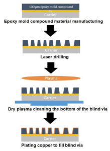
Traditional TMI mainly uses laser drilling to form the RDL by subsequent electroplating. However, during the laser drilling process, many filler particulates are generated and left on the surface of Cu. Cleaning is difficult and subsequent electroplating is affected. The more traditional way of cleaning is to use a wet chemical to remove these residues. Although the effect is very good, the chemical solution may damage the mold or dielectric material on the wafer surface.
In this study, CF4 and O2 plasma was used to clean up the residue after the laser drilling process. The gas composition and plasma treatment time were adjusted, and an optical microscope (OM) and energy dispersive X-Ray (EDX) were used to observe residues.
They found that after CF4/O2 plasma treatment, copper oxide was formed which needed to be removed by acetic acid cleaning. Then copper metallization was successfully plated along the mold compound via sidewall with either 20µm or 5μm filler particles.
IME – Status of Fan-Out WLP Line
IME has worked with industry partners to establish a fan-out wafer-level packaging (FOWLP) development line to address challenges to build broad FO WLP platforms to enable product and technology pathfinding for industry applications such as mobility, 5G, mm-wave, data center, and automotive. The development line can support different process schemes including the standard mold-first process flow and the RDL-first process flow approaches.
Mold-first is basically the well establish eWLB approach proven by many companies in volume production. The key concerns for this approach are die shift, die protrusion, and warpage. With various mitigation methods proposed, it remains one of the most cost-effective and simple approaches.
In RDL-first FOWLP, the RDL layer is processed first on a relatively flat carrier like a glass followed by chip attachment through the standard flip-chip-on-wafer process and mold encapsulation. As the chips are bonded and secured to the RDL layer, there is no issue with die shift or die protrusion. As the carrier is relatively flat, this approach supports fine RDL of 2µm or below. Multi-layer RDL of 2µm line and spacing up to 7 layers have been demonstrated on the IME line.
Integrated PoP
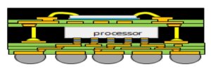
Application processor unit (APU) package-on-package (PoP) is widely used to achieve a low-profile configuration for smartphones. IME has further reduced the total package thickness by eliminating the solder joint required between the top memory to the bottom AP package. This is achieved through the integration of the memory chips directly on top of AP packaging in the FOWLP platform (Figure 3).
Embedded Fine Interconnect Package
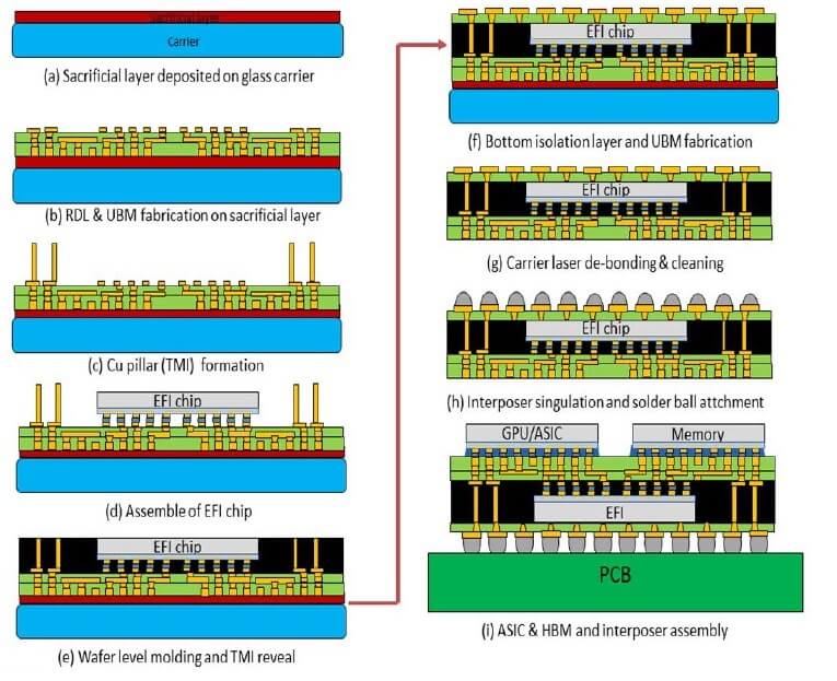
To enable further increase in chip-to-chip interconnection density requirements, a high-density Si chip with fine interconnect can be embedded in the mold compound layer in the RDL-first process flow as shown in Figure 4.
Antenna in Package
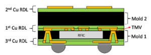
Antenna-in-package (AiP) is of interest for applications in 5G mm-Wave, mobility, and automotive. Integrating the antenna directly on the package has many advantages such as improved performance by reduced transmission losses and improved transmitter efficiency and short interconnection, smaller form-factor, and improved reliability. A unique solution allows a radio frequency (RF) chip in the face-up configuration for a thermal solution to be designed on the chip backside for improved thermal dissipation through the printed circuit board (PCB), as the top side is used for antenna transmission. A 10x10mm AiP package with an RFIC chip size of 4x4mm has been implemented with a 4×4 patch antenna for the 60Ghz WLAN application shown in Figure 5.
TSMC to do Packaging in Japan
While the US is “reshoring”, TSMC plans to set up a joint advanced integrated circuit packaging and testing plant in Japan at the invitation of the Japanese Ministry of Economy, Trade, and Industry (METI).
The report said that the joint venture is expected to be built in Tokyo. TSMC and METI are expected to sign a memorandum of understanding (MOU) and publicly announce the project in the near future. If the plan proceeds, it would be TSMC’s first overseas IC packaging and testing site. TSMC already has advanced IC packaging and testing plants in Taoyuan, Hsinchu, Taichung, and Tainan. This past November, TSMC’s board approved $3.5 billion for a foundry in Arizona.
As IFTLE has been noting, TSMC has moved aggressively into high-end IC packaging and testing to provide one-stop shopping services for clients who require advanced 3D package and testing technology.
For all the latest in Advanced Packaging stay linked to IFTLE………………………..