

Over its 17 years of existence, the IWLPC has morphed from a conference focused on wafer-level packaging to one basically focused on anything advanced packaging. It is organized by SMTA and Chip Scale Review. Let’s first take a closer look at some of this year’s virtual presentations by Samsung.
Samsung Keynote
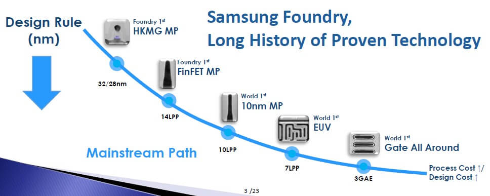
In the plenary presentation, Dan Oh, VP of Test & System Packaging shared his thoughts on “Trends, Challenges, and Opportunities in Advanced Packaging for a Smart Computing Era”. While Moore’s Law continues, performance gains are shrinking with the process and design costs rising. At 3nm Samsung will be moving to a gate-all-around GAA) architecture (Figure 1).
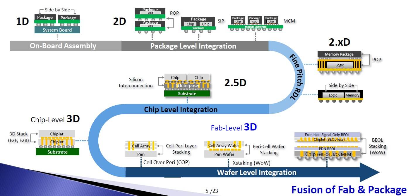
For high-performance computing (HPC) they see a move to silicon interposers, stacked memory and chiplet technologies / advanced packaging architectures, and a final evolution to a fusion of fab and packaging (Figure 2).
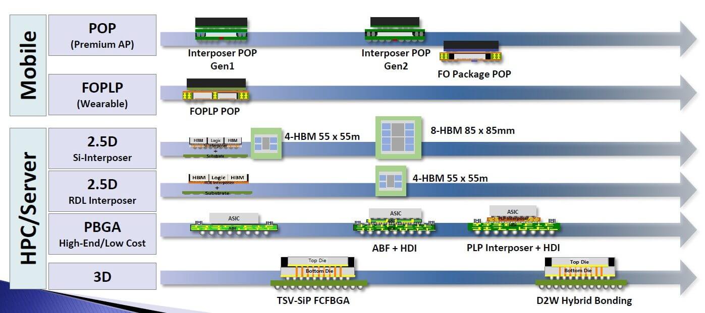
Oh noted that in today’s era, early-stage chip/package co-design is the key to success. He then laid out a plethora of Samsung packaging options as shown in Figure 3.
From his perspective advanced packaging design challenges center on:
- signal integrity
- power integrity
- thermal integrity
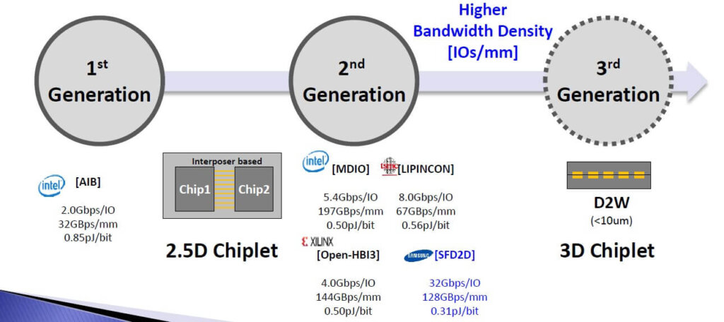
When it comes to the use of chiplets, as IFTLE has been telling you for a few years now, the communication interface appears to be the key to broad adoption. While Intel’s AIB has an early 1st gen solution, Oh sees Intel, TSMC, Xilinx, and Samsung adopting different interfaces. IFTLE feels this will greatly impede broad adoption and the ability to mix and match chiplets from different vendor sources.
Oh wonders whether we will be seeing chiplets replacing today’s high bandwidth memory (HBM) memory stacks. Since Samsung is the worlds leading memory supplier, I think we can safely say that they are probably determining the viability of this option.
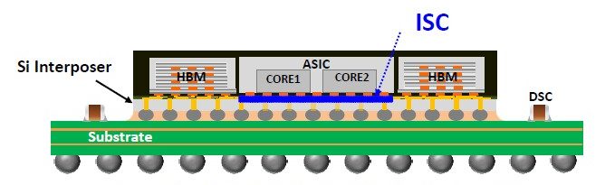
Oh sees the possible integration of high-density silicon capacitors (ISC). These ISC can provide ~10x cap density over standard MIM (metal/insulator/metal) caps. ISC can be embedded in the silicon interposer and due to its close proximity, will act as an on-chip capacitor (Figure 6).
Advanced Packaging Presentation
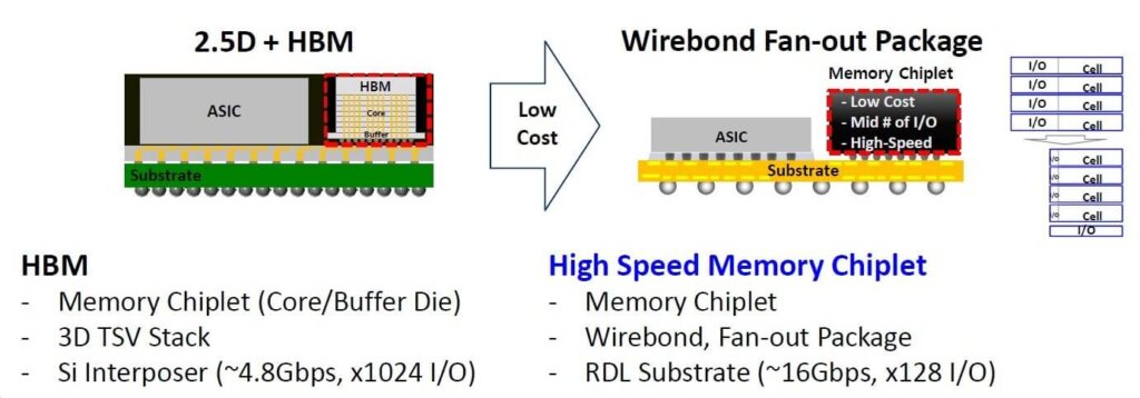
In a second Samsung presentation, Jae-Gwon Jang and co-workers presented a paper on “Advanced RDL Interposer Packaging Technology for Heterogeneous Integration”. HBM integration with logic dies at a system-level has been developed on a 2.5D system-in-package (SiP) platform with Si Interposer and through silicon via (TSV) but low/mid-end markets are sensitive to cost and thus 2.5D SiP with Si interposer becomes a concern due to its high fabrication cost. Samsung has developed an RDL Interposer package as a 2.5D package platform based on RDL-first fan-out wafer level package (FOWLP).

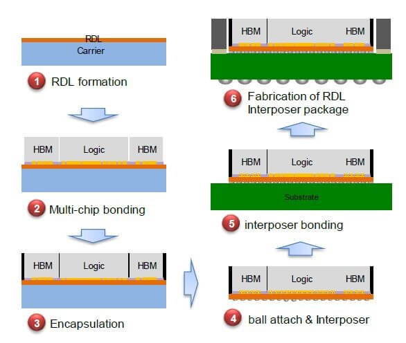
An RDL interposer package is fabricated using wafer-level manufacturing processes using the existing fab equipment. One can form the very fine pitch RDL patterns that are required for high-density interconnections between logic and HBM. In addition, Samsung contends that RDL has better design flexibility in terms of line width/space/thickness and dielectric thickness and via size. There are also various dielectric material candidates in the market, which provide options to achieve the best electrical characteristics. It is also beneficial for mechanical properties since CTE and modulus can be matched between RDL and substrate and, as a result, the package level thermal stress can be minimized for better package reliability. The process flow for their package is shown in Figure 7.
Samsung notes that it is important to select an electrically stable dielectric material to prevent any electrical leakage risk across the fine spaces. The most challenging factor in the assembly process was reportedly control of the interposer`s warpage due to the large substrate size and multiple chips.
The RDL Interposer has four-layer RDL to interconnect signals of one logic chip and four HBMs. Signal lines with fine pitch line-and-space are located on 1st and 3rd RDL layers and the other layers have ground and power layers. The fully completed 55 x 55 sq mm 2.5D RDL Interposer Package with 2/2 L/S consists of 5Multi-chips and Stiffener as shown below beside a cross-sectional image of the micro bump and C4 bump.
For all the latest in advanced packaging stay linked to IFTLE………………………………..


