

As a process geek, The Symposia on VLSI Technology and Circuits has long been one of my favorite conferences. The fact that it rotates between Kyoto and Honolulu adds a bit to its attractiveness. However, VLSI 2020, as with most, was held virtually.
Having attended a reasonable share of conferences and presentations this year, I think the IEEE and the VLSI committee did a great job of making this conference available to the attendees, as well as managing the number of speakers and keeping the conference running seamlessly, or at least it seemed that way to me. As a virtual conference, VLSI added a few features that I thought helped attendees get the most out of it and possibly attend some sessions that they may not have if they have attended in person.
One aspect that I particularly like was the executive sessions that the VLSI committee included. These sessions gave a quick two-minute overview, with essentially a live Q&A session, either by the moderators of the session or via online chat. This allowed attendees to get a quick view of the session, get their questions answered, and then decide if they wanted to hear the entire paper.
Moore’s Law Continues in 3D
The advanced CMOS Si session discussed the transistors of the future. Currently, FinFETs are considered to be the transistor of choice through the 5nm technology node. Past 5nm it appears the transistor of choice will move to stacked nanosheets. TSMC and CEA-Leti presented on nanosheet gate all around (GAA). It was a bit surprising that there were only two papers on this topic, and that none of the other logic manufacturers or research groups contributed to it. CEA-Leti presented on a 7-layer GAA structure (Figure 1). Sometimes the lack of industry papers means that they are getting close to high volume manufacturing and they don’t want to tip their hand as to what they are doing.
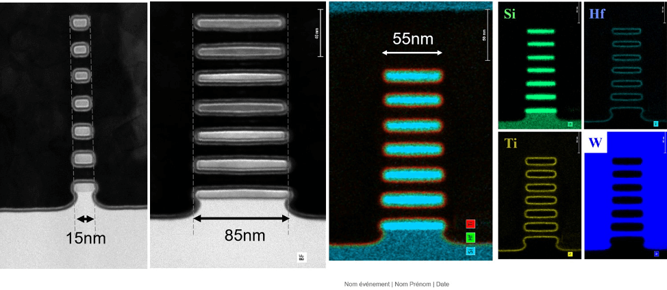
The 7-layer GAA will lead to sub 5nm technology nodes with transistors that have improved gate control and higher DC performance over FinFETs, according to the author Sylvain Barraud. The complexity of processing the GAA nanosheets is complex, so it will be a few more years before this technology is in mainstream production.
One of the possible alternatives, or it might be better to say the evolution of nanosheets, are monolithic transistors. In Figure 2, the IMEC paper presented by Sujith Subramanian demonstrates the transition from nanosheet transistors to forksheet to complementary transistors (CFETs), where the NMOS nanosheet FET is stacked on top of the PMOS FinFET. The argument is that the stacked transistors will significantly reduce the area needed for future technology nodes, thus enabling the continuation of “Moore’s Law” increasing the number of transistors per unit area.
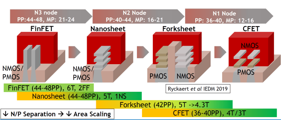
The electrical data looks promising, but the authors have yet to build the entire 3D device. There is the PFET data and the NFET data, but no CFET data; so there is the possibility that the thermal processing of the NFET might have some effect on the PFET. A great deal of work is still needed before this will get to high volume manufacturing, but work by CEA-LETI and IMEC in this space are showing a great deal of promise.
One of the process areas that amazes me in the monolithic 3D integration is the advances in low-temperature epitaxy without anneal. Getting decent device characteristics with epi grown at 525°C is mind-boggling to this old batch epi person. Some subsequent monolithic papers that use laser annealing processes for doping and material annealing suggest that monolithic manufacturing will be mainstream relatively soon, as laser annealing enables the process flow to manage the thermal budget, such that there is little if any damage to the base device, as presented in the CEA-Leti paper on building sequential CMOS devices at 525°C or less. The low-temperature process techniques have opened the door to combining GaN transistors with silicon transistors, as shown by Intel, which can be advantageous in the power semiconductor, and communications devices as demonstrated in the Intel paper using a layer transfer technique for the Si layer on top of GaN transistors. Low-temperature processes were then used to manufacture the Si transistor with no impact on the GaN transistors.
In the distant future, once 3D integration gets neuromorphic compute under control, quantum computing or qubits will enter high-performance computing. While quantum computing will replace some of the high-performance compute applications unless quantum computing can be developed at room temperature, the use in everyday applications such as a mobile phone is unlikely, as carrying around a bottle of liquid nitrogen isn’t really feasible.

More than Moore
3D Packaging or monolithic semiconductors are increasing in importance for both high-performance computing (HPC) in AI learning, and sensors for the IoT. The need for more computing power combined with memory is critical for reducing AI learning time and potentially reducing both the time and energy needed in the learning phase of AI.
In the sensor space, being able to successfully combine, either in package or silicon, improves the performance and can reduce the power of the sensor package. It is also possible to add some additional compute power, thus creating an integrated low power nearly stand-alone sensor system. There was considerable information on the above in the short courses. The goal or challenge is to place as much compute power with the optimum memory power in the same package for AI or HPC applications.
While there was a good deal of information on the heterogeneous packaging in the short courses there were only a few papers on the topic in the conference sessions. TSMC presented one paper in the heterogeneous integration on the HPC aspects of packaging using 7nm processors and demonstrating how to effectively deliver power to the processors and chiplet package. CEA-LETI presented on their ExaNode process for building systems for HPC applications.
As memory is key for HPC figuring out how to increase the amount of DRAM available to the logic in heterogenous packaging is key. In the 3D packaging session, the focus was on memory bandwidth as a key issue for high performance and neuromorphic computing applications. CH Tsai of TSMC presented on the company’s system-on-integrated chip (SoIC) bumping process that will eventually allow for 16 DRAM to be combined into the high bandwidth memory (HBM) stack. Nine is the current technology, and the paper presented 12 memory layers. The micro bump process reduced thermal performance by 7% and 8% respectively in the 12 and 16-layer HBM.
Norio Chujo of Hitachi presented on a bumpless build cube (BBC) wafer-on-wafer (WOW) which uses a through silicon via (TSV)-to-TSV contact eliminating the bumps completely. Chujo used a wafer-level stacking technique that created a 9-layer HBM stack. Chujo is proposed that a 32-layer stack is possible using the bumpless technique. The paper claimed that by eliminating the bumps, the capacitance was 1/20 of a conventional bumping process.
As I close, if I use the VLSI conference to help predict the direction that process technology will move in the next several years. It appears that the industry will continue to focus on smaller faster transistors to continue to facilitate a form of “Moore’s Law”. However, packaging will become increasingly important in the area of both sensors and HPC, as the packaging engineers figure out how to put the devices together in the optimum configuration as business continues to move into the digital realm. ~ D. Freeman


