
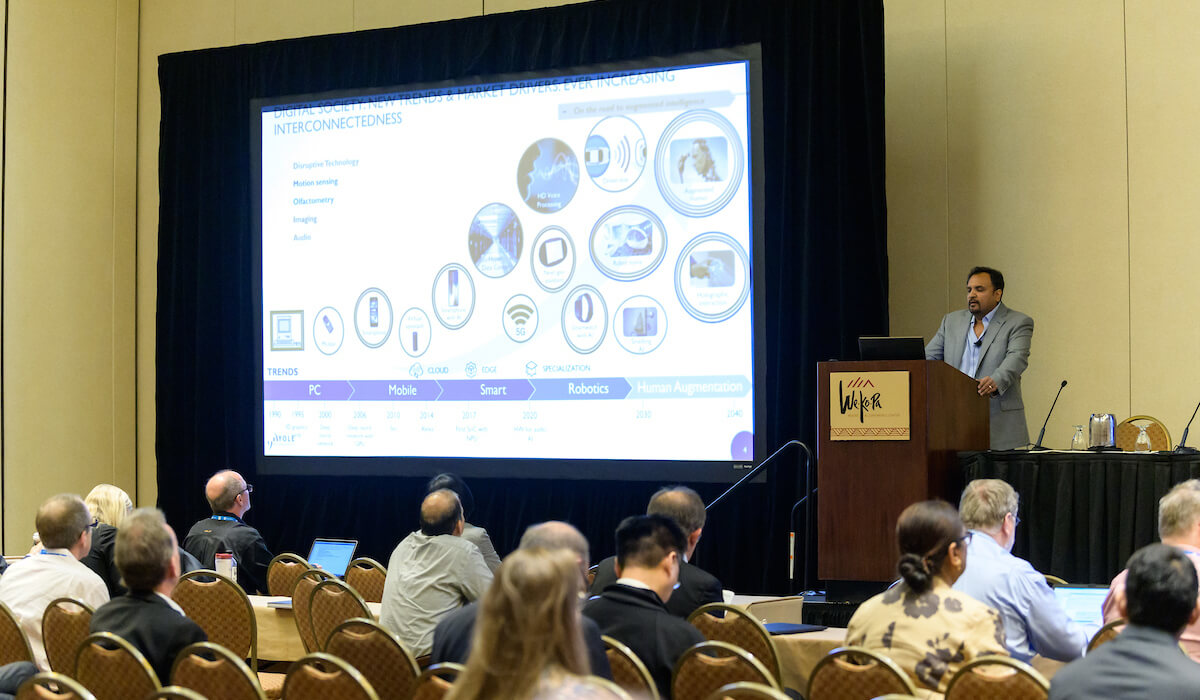
At the recent IMAPS Device Packaging Conference, Yole discussed how advanced packaging is leading electronics into the next decade. As you have heard from IFTLE for many years now, scaling is falling into the background as advanced packaging is taking the lead in determining the majority of new product innovations.
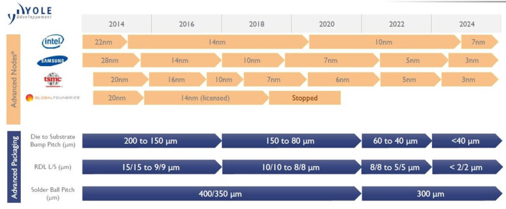
The following tech roadmap is a nice summary of state-of-the-art (SOTA) technologies over the last decade (Figure 1).
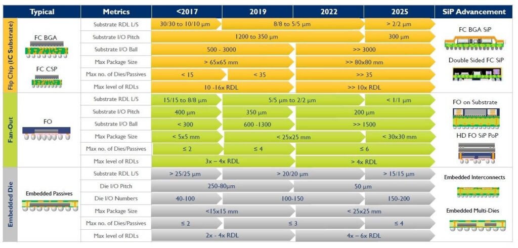
Similarly, their roadmap for system-in-package (SIP) technologies projects out to 2025 comparing ground rules for SOTA flip-chip ball grid array/chip-scale packages (FCBGA/CSP) vs fan-out (FO) packages vs embedded packages (Figure 2).
(These projections are based on an average of the different technologies available in the market.)
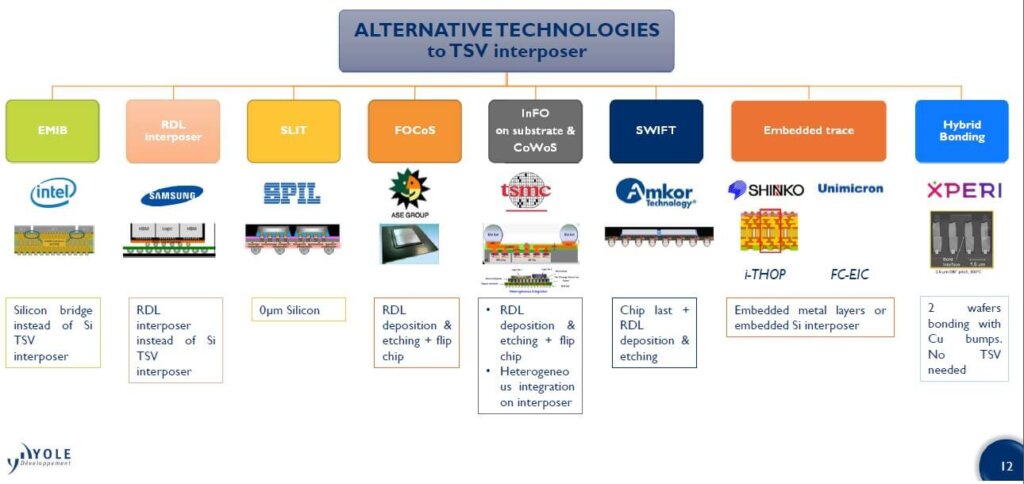
They also examined the technologies being developed based on non through silicon via (TSV) process flows to compete with silicon interposer TSV substrates (Figure 3)
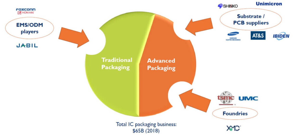
While packaging and assembly was traditionally the domain of outsourced semiconductor assembly and test (OSAT) service providers and integrated device manufacturers (IDMs), foundries, substrate/printed circuit board (PCB) suppliers and electronic manufacturers (EMS)/originial design manufacturers (ODMs) are entering the business and trying to cannibalize the OSATs positions. In the future IFTLE thinks this will also lead to M&A activity from these new players eager to get a foothold in the advanced packaging market segment (Figure .
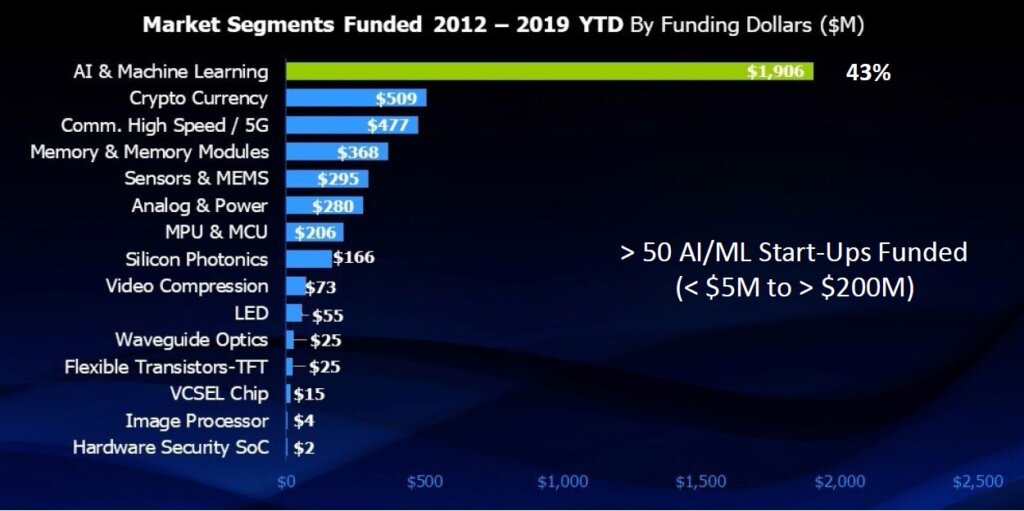
In the ASE presentation on how “Integration Technologies are Transforming the World” they pointed out that nearly half the VC funding for electronics is being poured into artificial intelligence (AI) and machine learning (ML) and that 2.5 and 3D packages are in fact enabling performance hardware for such deep learning applications.

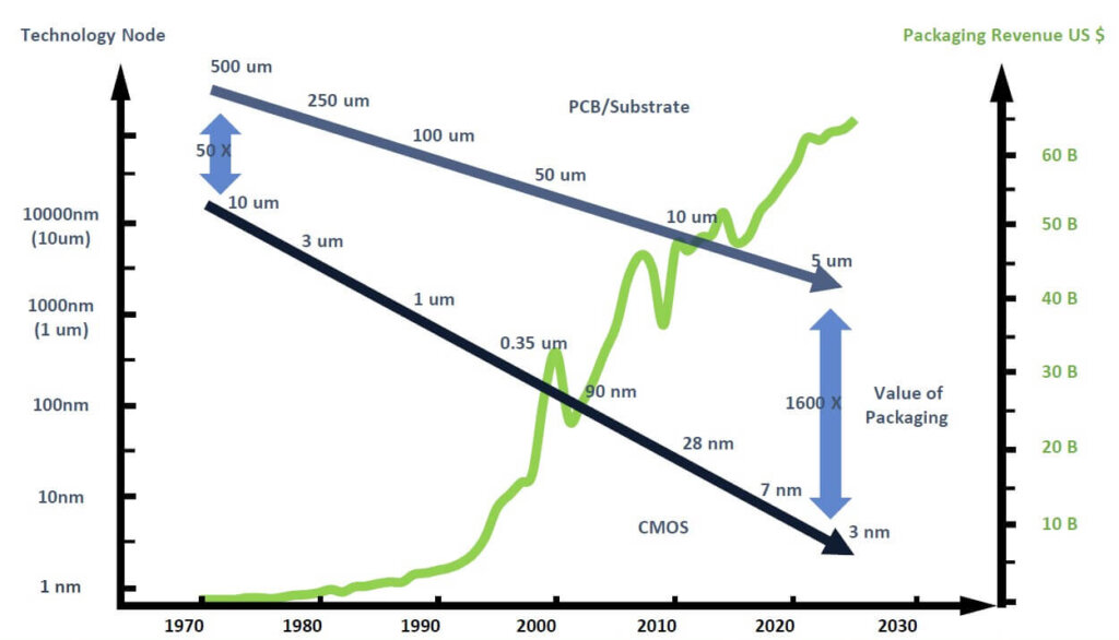
The following graph was used to show how the value of semiconductor packaging is increasing.
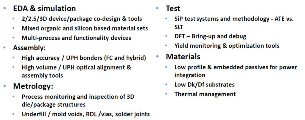
Importantly they listed the ecosystem support that will be required to move forward.
For all the latest in advanced packaging stay linked to IFTLE………………………………………………


