
 In the latest issue of IMAPS “Advancing Microelectronics” magazine (Nov/Dec 2019) Lei Fu and his colleagues at AMD published an interesting article on copper pillar bump (CPB) development for 7nm node devices. Let’s take a look at what they reported.
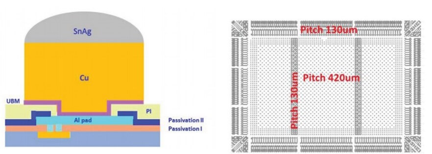
In contrast to 14nm/16nm nodes, which used 150µm bump pitch coming out of a die, for 7nm node the industry is targeting 130µm bump pitch for high-performance devices. With the smaller bump pitch, conventional SnAg lead-free solder bumps are not suitable because they are prone to solder bridging and bump shorts. CPBs can solve the challenges of tighter bump pitches, but the challenge with CPBs is their interaction with extreme low-k (ELK) dielectric in the underlying back-end-of-line (BEOL) layers. CPBs are much stiffer than solder bumps. Due to the CTE mismatch between silicon and laminate substrate, the stiff CPB will transfer stress to the silicon BEOL layer, potentially causing ELK cracking. This can affect reliability. Thus, the copper pillar design and subsequent laminate assembly process needs to be carefully optimized.
AMD has developed a chip package interaction (CPI) test vehicle to evaluate the impact of various variables on reliability. The test vehicle is built with the same ELK material, in the same 7nm process, with the same substrate and assembly process. Daisy chains have been designed through BEOL layers for validating BEOL integrity. 130µm bump pitch in the periphery area and large bump pitch at the die center have been defined as shown in Figure 1. JEDEC standard tests (Preconditioning, HAST, TCJ, and HTS) are used as criteria for qualification. Accelerated thermal cycling (ATC) is used to assess copper pillar interactions with ELK layers.
UBM Size Effects
CBP can transfer stress to the ELK layer causing cracking of ELK (white bumps). Larger UBM is one of the effective ways to spread the stress across the bump area. AMD found that the results indicate that ELK peeling stress is reduced 18% with 85µm under bump metallization (UBM) vs 75µm UBM.
Copper Pillar Height
Cu pillar height sets the standoff height after assembly and standoff height is known to be more reliable. However, the tall pillars can increase ELK stress without underfill. They found that bump stress increases 22% from 20µm to 40µm pillar height, and 15% from 40µm to 100µm.
Bump Pitch for 7nm
Reducing bump pitch from 150µm to 110µm lowered ELK stress by 69%. They conclude that decreased pitch results in more support at the die corners thus reducing stress concentration on individual bumps and reducing stress on the ELK layers.
Die Thickness
By using thinner chips, the effective coefficient of thermal expansion (CTE) difference between the chip and package substrate can be reduced because the volume of the chip is reduced. The die stiffness is also reduced. The net effect is an expected reduction in stress. They found ELK peeling stress decreases 40% with die thickness from 750µm to 200µm.
Dielectric Opening
PI acts as a stress buffer layer and plays an important role in ELK stress reduction. Geometric parameters associated with PI are investigated to find ways to lower stress on the ELK layers. They found that ELK peeling stress increases 16% with a PI opening increase from 20µm to 40µm and rationalized that the smaller PI opening offers greater padding to act as a stress buffer layer.
Aluminum Terminal Pad Diameter
Al is widely used on the die as a bump terminal metal to reduce white bump failures. ELK peeling stress decreases with increasing pad diameter. This is because a larger pad provides a larger area for stress dissipation and energy absorption.
The optimized bump geometry for 7nm was determined based on the above modeling results and these ground rules applied to the 7nm CPI qualification.

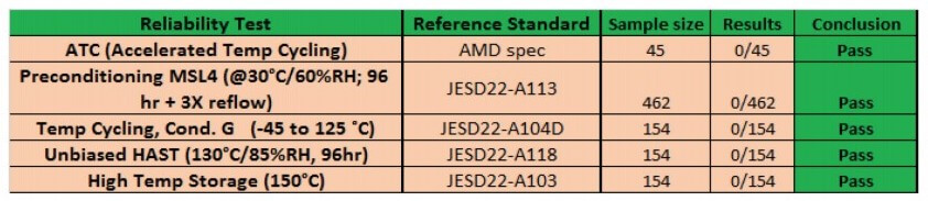
The standard JEDEC tests with selected conditions (preconditioning, TCG, UBHAST, HTS) were used for Cu pillar development for 7nm CPI qualification. Test results, shown below. Indicate that optimized Cu pillar bumps passed CPI qualification. They indicate that Cu pillar bump design rules pass the reliability tests. These results have reportedly been implemented in AMD’s 7nm products (Table 1).
Electromigration
Electromigration (EM) has received a lot of attention due to high-performance computing and gaming requirements. The evaluation of the Cu pillar bump EM performance is required to help designers decide the max current that can be applied to the device.
An EM test vehicle (TV) was designed and built. An EM test system has been set up to test optimized Cu pillar bumps. Results are shown below for EM test results of SnAg bump and a Cu pillar bump under the same test condition (Figure 2).
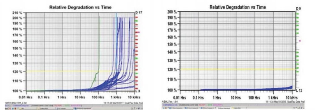
There are a few early failures for SnAg bumps. Many units start to fail after 1000 hours and most of the samples fail at 10k hours with the test condition of 0.6A/140°C. Looking at Cu pillar bumps, no unit failed in 10K hours under the same test condition. It can be concluded that a Cu pillar bump has much better EM performance than a SnAg bump.
For all the latest in Advanced Packaging stay linked to IFTLE ………………………………
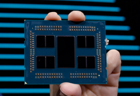
Feature image: AMD’s Threadripper built on 7nm manufacturing process. (Courtesy of AMD)


