

Beyond HPC
High-performance computing (HPC) has become an important tool for areas that generate high volumes of data. While today’s HPC is already powerful, many scientific and industrial challenges require even more computing power, for instance, drug discovery and material design. Thus, the global drive for exascale (1018) computing.
HPC systems that currently dominate the market are based on processors with high, per-core processing power and memory bandwidth. A comparison between various past, present and emerging HPC architectures as developed in the European Exanode program is shown below [link]. They conclude that “main-stream x86 platforms show high HPL performance that increased significantly in each generation. ThunderX shows the best performance of the ARM platforms. We detect a large gap between the main-stream x86 and emerging ARM platforms, e.g. Haswell provides 8.9x higher HPL performance then ThunderX servers. This performance difference can be at least partially explained by a need for software optimized for ARM platforms.”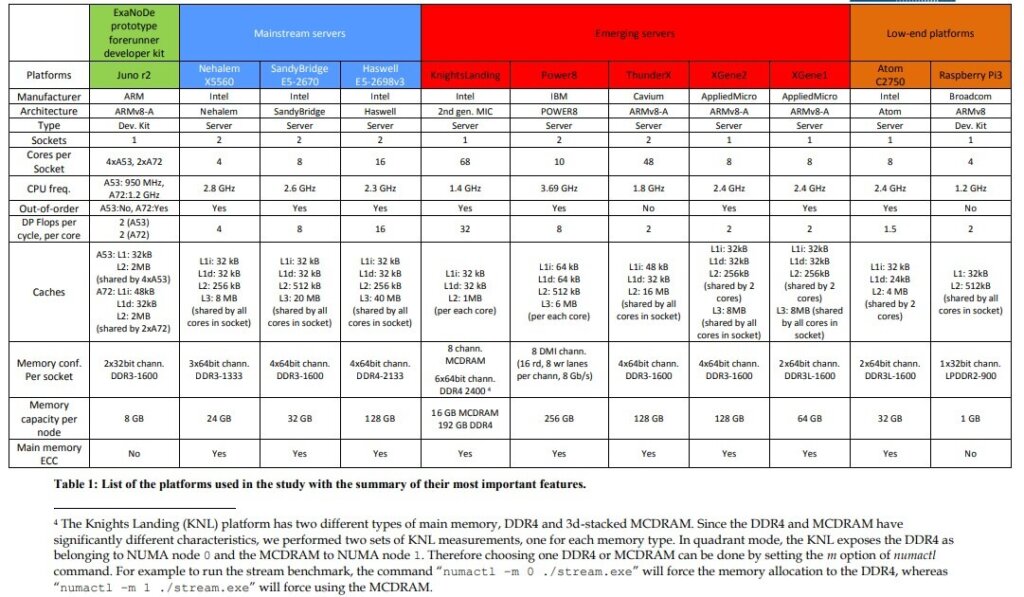
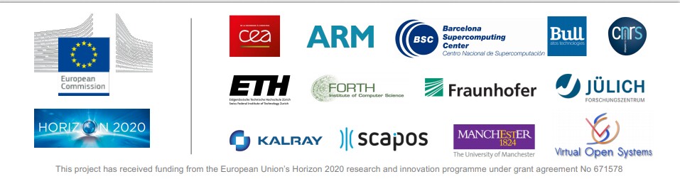
Thirteen partners in Europe were involved in the pan-European exascale computing collaboration funded (8.6MM Euro) under the European Commission’s Horizon 2020 program. The participants are shown below.
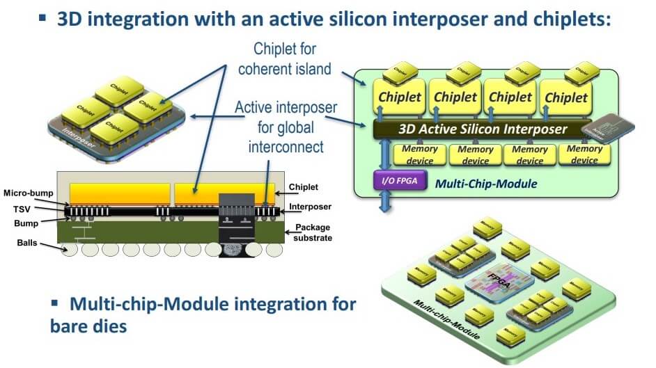
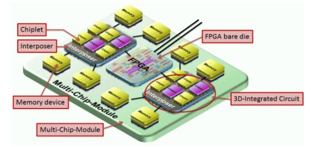
Below we see the Exanode integration approach using interposer and chiplet technologies.
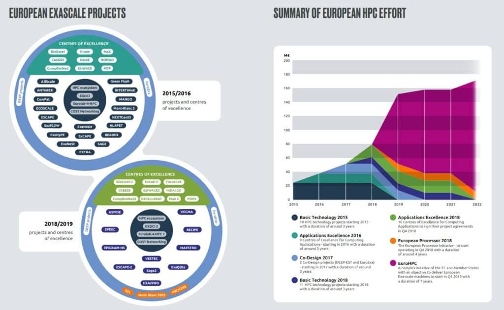
A complete list of European Exascale computing projects ( ~ 200MM Euro) is shown below. Details can be found here.
Prototype Delivered

The European ExaNoDe project has recently wrapped up and announced that they have built a complete prototype of a 3D IC exascale compute node containing FPGAs, HBM2 memory, and 7nm Arm chiplets with active interposers. As you can clearly see, and as IFTLE has been predicting now for some time, advanced packaging is instrumental in being able to deliver such systems.
The concept diagram in Figure 5 shows a large multi-chip module (MCM) composed of an FPGA in the middle, surrounded by two of the active interposers and eight HBM2 memory stacks. The interposer itself contains six chiplets, based on 7nm Arm cores. The chiplets delivered with the prototype, which were manufactured by STMicroelectronics’s FD-SOI 28nm process, only contain communication logic for the interposer-chiplet complex plus a specialized hardware block for accelerating convolution neural network (CNN) computations.
Reports on the exanode design guidelines have been reported here.
For all the latest in Advanced Packaging stay linked to IFTLE…………………………………


