
In this IFTLE post, we continue our look at presentations from the 2018 EPTC Conference…
Ultratech / IMEC / JSR – 1µm RDL
Ultratech, IMEC and JSR discussed “One Micron Damascene Redistribution for Fan-Out Wafer Level Packaging using a Photosensitive Dielectric Material”. This study compared the creation of 1.0μm RDL structures by a damascene process utilizing a photosensitive permanent dielectric material with the traditional semi-additive process flow. The advantage of the damascene photosensitive dielectric approach is that the Cu overburden removal does not affect the quality of the embedded Cu lines. In comparison, for a semi-additive process, the Cu seed etch does affect the final dimensions of the RDL lines. Damascene processing reportedly also results in a flat wafer surface, which greatly improves the lithographic performance for subsequent layers. Finally, in the damascene process flow, the RDL Cu line is surrounded on the sides and bottom by Ti which provides a Cu diffusion barrier for enhanced reliability. They report significant electrical results advantages for the damascene process compared to the semi-additive process (Figure 1).
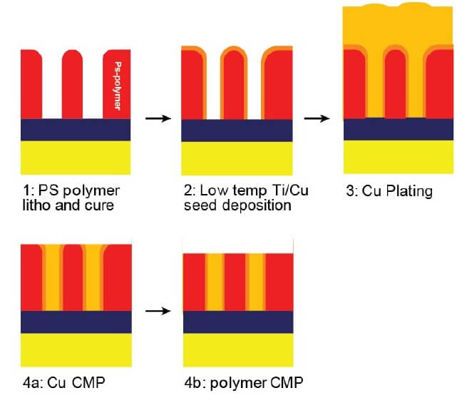
The damascene process relies primarily on the patterning of the dielectric material to define the final feature size. The CMP process to remove the overburden after Cu plating is also important but does not affect the quality of the Cu lines.
IME A Star
IME A Star gave several presentations at the conference. Here are a few of the topics they examined.
FOWLP Die Shift and Die Protrusion issues
Lim and co-workers at IME A Star discussed “Comprehensive Study on Die Shift and Die Protrusion Issues during Molding Process of Mold-1st FOWLP”. Fan-out wafer-level packaging (FOWLP) is a viable low-cost, small form factor packaging technology. However, warpage largely induced by the molding compound becomes a challenge during fabrication. Die shift from the original bonded position during encapsulation can be affected by material expansion rate, dragging force during encapsulation and the mold compound shrinkage properties. Die protrusion is the step height measured from the die surface to the mold compound surface. The height differences between the die surface to the mold compound surface impact the co-planarity issues faced in the stringent requirement of finer pitch and width of the RDL lithography process. This die protrusion will greatly impact on the RDL breakage, shorting and open failures (Figure 2).
IME evaluated 3 different configurations of FOWLP Mold-1st packages to study the impact of the configuration and process parameters on die shift and die protrusion during the assembly process. The authors successfully achieved die shift of ±15μm for 3 different molded fan-out wafers at ±10μm die protrusion. They conclude:
- Lower bonding force caused higher die shift as compared to using medium and higher bond force.
- Die protrusion increases at higher bonding force.
- Selection of optimum bonding force is critical to allow minimum die shift and die protrusion for better smooth alignment integration during the lithography process and no distortion of the fine metal layer width during the fabrication process.
Copper Overburden Removal
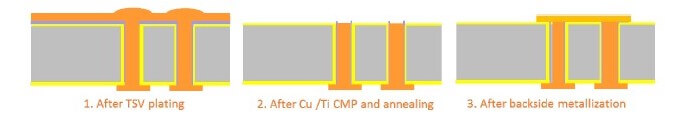
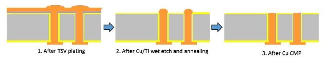
In another presentation, IME discussed “Development of Cost-effective Copper Overburden Removal for Via-last TSV Fabrication”. The conventional approach to remove the copper overburden is by chemical mechanical polishing (CMP). Cu annealing can be done before or after CMP. It’s reported that CMP uniformity on a temporary bonded wafer can be improved when Cu annealing performed after CMP. A schematic to illustrate this integration flow is as shown in Figure 3. To ensure the metal layer is thoroughly removed after CMP, over-polishing is needed, which can result in as much as 5µm of Cu dishing at the surface. Large Cu dishing can cause backside metallization issues.
The second approach to remove Cu overburden is to replace CMP by wet etch. A drawback of this approach is that Cu protrusion can cause poor RDL flatness, which will affect TSV resistance and reliability. The third approach to remove Cu overburden is to combine wet etch and CMP, as shown in Figure 4. This approach reduces Cu dishing and protrusion, improves TSV surface flatness and electrical performance while keeping the process cost low. A drawback of this approach is that fabrication throughput is slightly lower and the cost is slightly higher than the CMP-less wet etch approach.

Development of Antenna for FOWLP
This paper describes the development of a FOWLP package that uses mold encapsulation to form the antenna element. The FO-WLP package is designed with a target frequency of 60GHz for wireless local area network (WLAN) applications. A cross-section of the antenna package is shown in Figure 5.
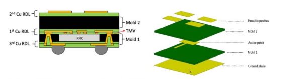
The radio frequency integrated circuit (RFIC) chip consists of the multi-channel transceivers embedded within the first mold compound. 1st Cu RDL is used to route the interconnections between RF signals, power and control signals from the I/O’s of the chip to the fan-out region of the mold compound and also forms the active antenna patches. A second mold compound encapsulates the active antenna patches and a second metallization is processed on top of the second mold to form parasitic patches. There are no electrical connection paths between the 1st and 2nd Cu RDL. The unique features of this design are that the antenna performance can be adjusted and optimize by varying the thickness of the second mold compound.
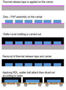
steps (a) to (k) in Figure 6 illustrates the fabrication flow of the antenna in the FO-WLP. The device chips were picked and placed device face-down onto metal carrier laminated with double-sided adhesive tape. An epoxy mold compound encapsulates the chips to form a reconstructed wafer. Upon completing the 1st Cu RDL, a second layer of epoxy mold was molded on top of the Cu RDL. A backgrinding process is implemented to remove excess over-mold to attain the desired thickness; which is a critical factor to the performance of the antennas. A 2nd Cu RDL was processed over the second mold to act as the parasitic patches. After completion of the 2nd Cu RDL, the wafer was flipped and bonded with adhesive temporarily onto a glass carrier for the back-side RDL processes. The back-grinding process is conducted to remove the over-mold at the backside of the wafer; to expose the dies. A laser drilling process was used to form blind vias to enable electrical routing between 1st Cu RDL and the 3rd Cu layer. After balling, The reconstructed wafer was de-bonded from the glass carrier and the adhesive removed. The reconstructed wafer is then diced into individual packages and assembled to a PCB.
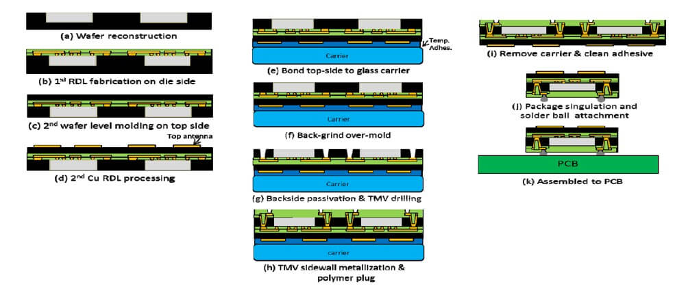
Laser drilling was performed from the wafer backside to create blind vias that terminate on 1st Cu RDL. A UV laser was used for the drilling. A 2-steps laser via drilling recipe was implemented; starting with high fluence laser to remove bulk mold compound and low fluence laser to remove mold residue on the copper pads.
For all the latest in Advanced Packaging stay linked to IFTLE……………….


