

Dense materials that exhibit high thermal conductivity are abundant in nature: think copper, think diamond, think silicon. And porous materials with low thermal conductivity also exist, or are easily fabricated: think polyimide, for example, or think of the various porous xerogels.
But dense materials that are also thermal insulators, or porous materials that are good thermal conductors? Those are horses of different colors not often seen in nature, and they are the subject of much interest and work by members of the Stanford University Department of Mechanical Engineering, chaired by Professor Kenneth Goodson, who presented a fascinating talk on the subject of thermal metamaterials at the MEPTEC/IMAPS Lunch at SEMI HQ in Milpitas, CA, on Wednesday 09 May 2018.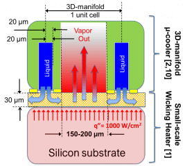
There’s cold, there’s warm, there’s heat, there’s Phoenix-area “It’s a dry heat,” and then there’s NanoHeat, the focus of Professor Goodson’s NanoHeat Lab, which studies heat transfer in electronic nanostructures & packaging, microfluidic heat sinks, and thermoelectric & photonic energy conversion devices, focusing on fundamental transport physics, among other aspects of the subject.
Who would this work interest? Semiconductor, energy, and automotive companies, for a start, including Intel, Google, Analog Devices, IBM, Bosch, Raytheon, and Toyota, to name a few, looking to solve thermal issues in server applications, consumer electronic products, vehicles, and defense systems.
As for practical results, consider these achievements developed by the lab: breakthrough heat spreaders, microfluidic heat sinks, and thermoelectric waste heat recovery and battery microcharging.
And following along with the (misattributed) quote from W. Edwards Deming, namely that “If you can’t measure it you can’t manage it,” the Stanford NanoHeat Lab also has a focus on developing and applying better instruments and techniques for thermal metrology including observing and measuring micro & nano conduction & convection.
Just what are metamaterials? According to Professor Goodson, metamaterials are materials and structures engineered to have properties that are not found in nature. Metamaterials are assembled from stacks or sheets of repeating units, at dimensions below a targeted mechanistic scale, in order to produce unique interactions with electromagnetic or photonic signals, or with acoustic signals, as a result of the structural properties of the metamaterial. (“Forced” intercalation is a second approach.)
 Or, as with our consideration here, to produce unique combinations of density, porosity, and thermal conductivity.
Graphene, said Professor Goodson, is an example of a metamaterial that is dense but not particularly thermally conductive and therefore can be usefully employed in an application such as this one: “Energy-Efficient Phase-Change Memory with Graphene as a Thermal Barrier.” (Stanford and Samsung, in NanoLetters, 2015.)
But the eye-catching work, at least to me, is in the other direction, with porous materials that conduct heat well.

Metal inverse opals in general, and more specifically copper inverse opals (see “Quasi-ballistic Electronic Thermal Conduction in Metal Inverse Opals,” from Stanford and the University of Illinois, also in NanoLetters, 2016), are metamaterials with just that special combination of low physical density and high heat conductivity that can be made to work well as heat spreaders in microfluidic-based heat removal structures for high power / high power density applications such as high frequency radar, renewable power generation and electric vehicles, and high performance computing. (More about that in “Extreme Two-Phase Cooling from Laser-Etched Diamond and Conformal, Template-Fabricated Microporous Copper,” in Advanced Functional Materials, 2017.)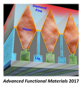
Diamonds and opals are part of a queen’s ancient riches, but graphene, and copper inverse opals, thermal metamaterials, are treasures of a sort themselves, and their current use in thermally demanding applications extends the long tradition of research at Stanford University on high performance heat exchangers, dating back to the early 1980s work by Kays and London, and by Tuckerman and Pease.
Today, the result of Stanford’s work with nanostructured copper bilayers and phase separation microfluidic chambers helps GaN-based HEMT radar electronics and MW semiconductor lasers deal with local power densities exceeding 30kW/cm2. And in your home or office, can be found as the heat sinks in Apple G5 workstations.
Further proliferation is sure to follow.
From Santa Clara, CA, thanks for reading. ~PFW


