
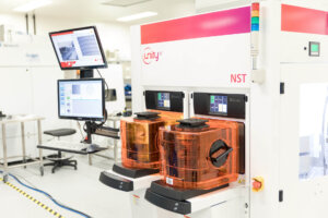
 Grenoble, France, March 14, 2017 – UnitySC, a wholly owned subsidiary of FOGALE Nanotech Group and a leader in inspection and metrology solutions for advanced semiconductor packaging, today introduced its new NST Series at SEMICON China in Shanghai. The NST Series is the world’s first non-contact metrology solution for accurately measuring the nanoscale surface topography of semiconductor wafers in high-volume manufacturing. The new platform enables higher wafer yields and throughputs and targets advanced processes being implemented for next-generation image sensor and memory technologies.
The ever-increasing performance requirements of today’s advanced semiconductor devices are driving the need for accurate, high-throughput in-line metrology. This is true for Cu CMP processes, pre- and post-Cu-to-Cu wafer hybrid bonding processes, as well as any type of front-end CMP and etch processes, all of which are necessary to enable the semiconductor industry’s move toward more efficient manufacturing.
“We developed the NST Series in response to the needs expressed by the industry and our customers,” said Gilles Fresquet, CEO, UnitySC. “The first tool was delivered in late 2016 to a key customer and partner and is in operation. We foresee significant shipments of this series this year. We believe it is a game changer in process control capabilities that will impact throughput and yield for all semiconductor profiling applications, and particularly advanced CMOS image sensors and 3D memory stacks.”
“The CIS industry was the first to directly leverage the development of 3D hybrid bonding techniques. According to our latest technology and market analyses, the significance of this hybrid bonding technology will exceed $1 billion USD in 2017 and will double the CIS market CAGR at an expected 20% until 2022,” said Pierre Cambou, Activity Leader, Imaging at Yole Développement. “With its new NST Series nanotopography metrology platform, UnitySC is directly addressing this growing market.” (1)
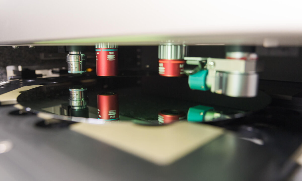
UnitySC’s NST Series semiconductor measurement equipment surpasses conventional optical interferometry by not being impacted by transparent layers. The NST Series extends beyond contact profilometry into the atomic-force-microscope-level performance. Contactless full-field profilometry at resolutions down to 0.1nm captures artifact-free area scans to deliver critical information much faster than existing solutions. A streamlined preparation process eliminates the metal deposition step after Cu chemical mechanical planarization (CMP) that is required by competing platforms to control wafer surface quality before the hybrid bonding process, thereby reducing wafer scrap and delivering higher yields. Additionally, NST is the only metrology platform that offers overlay capabilities for post-bond metrology in Cu-to-Cu hybrid bonding applications.
The NST Platform is now available in two configurations:

- The NST XP system provides versatile, high-speed and high-precision non-contact, full-field profilometry for single-die or multi-die surface topologies. It can perform a wide array of measurements, such as dishing, erosion, CD, step height, deep trench, and roughness.
- The NST Bond platform is a complete metrology solution for hybrid bonding, combining the NST XP’s capabilities with additional features for high-resolution measurement after the Cu CMP and Cu-to-Cu bonding processes, including in-plane and out-of-plane overlay.
UnitySC is exhibiting at SEMICON China, March 14-16, 2017 at the Shanghai New International Expo Centre in Shanghai. Please stop by booth #5375 in Hall W5 to learn more, or email Yann Guillou to arrange a meeting.
- Source: Status of the CMOS Image Sensor Industry 2016: New Market and Technology Dynamics report, Yole Développement, 2016.
About UnitySC
UnitySC is recognized worldwide as a key player in inspection and metrology, combining advanced technologies in automated optical inspection and 3D imaging with microscopy, temporal-mode interferometry, and spectrometry, which enables customers to deliver higher yields and faster time to market. Customers include the largest foundries, integrated device manufacturers, outsourced semiconductor assembly and test service providers, and R&D centers. The company provides standard and customized solutions adapted to specific industrial needs and constraints, enabling a new era in process control. Headquartered in Grenoble, France, the company maintains offices in Taiwan and is supported by a network of representatives and distributors. Learn more at unity-sc.com.


