
The Great Miniaturization … SEMI/MEPTEC Conference Nov 10 & 11, continued from Part 1.
Wednesday morning started with a IC packaging session focused on my favorite subject: Multi-die Integration.
Trevor Yancey, who recently joined Jan Vardaman at TechSearch International, talked about the IoT and gave an example for how the many sensors on a manufacturing floor will minimize downtime, improve quality, save energy, increase throughput and lower unit cost. He also showed how sensors will enable autonomous driving and assure both passenger- and pedestrian safety (Figure 1). Yancey also talked about the many IC package types available and the rapid unit growth they project for multi-die FOWLP.
Xilinx’ Ivor Barber demonstrated why and how combining multiple dies in an IC package, all using a high yielding, mature technology, is more cost-effective than integrating the same number of transistors using the next, still immature process node. This concept allowed Xilinx to leapfrog with their Virtex-7 2000T the competition. He also highlighted that integration of heterogeneous dies in an IC package offers many benefits, as proven with the Virtex-7 H580T.
Vincent Liao from ASE focused on development challenges for cost effective multi-die integration. He started out with demonstrating how multiple dies complicate EMI shielding, then showed how many ways ASE has developed to mitigate and eliminate EMI problems. After talking about how to suppress radiation, Liao talked about how ASE achieves the opposite: Embedding efficient and cost-effective on-chip antennas. Fitting the session title “multi-die integration” Liao also covered ASE’s many ways of integrating multiple dies in a single- or double-sided package or module.
Wednesday’s late morning session focused on SIP and Modules
Analog Devices’ Mike DeLaus presented ADI’s perspective of and strengths for heterogeneous integration. (See Figure 2)
DeLaus stated that ADI is transitioning from developing ICs to creating heterogeneous modules. They combine ADI’s die-level analog IP with digital dies from 3rd parties, utilizing multi-die packaging technology from a partner. He showed wafer-level integration of ASICs and MEMS, also how they integrate optical sensors and GaAs RF circuits into such a module.
Harrison Chang also showed, like Ou Li in the morning, the breath of ASE’s packaging technologies and demonstrated on three generations of LTE modems how ASE was able to contribute to cost- and area reduction, two essential differentiators. Chang showed that ASE reduced the LTE modem’s component count from 372 to 218 and area from 23×26 to 15×15 mm. He was the first presenter to emphasize so far untouched topics: Design tools, test and failure analysis as essential capabilities for reaching cost-effective volume production.
Jawbone’s Ilyas Mohammed added a consumer/wearables perspective. He showed their range of biometric devices and emphasized the importance ultra-low power dissipation (20-30 uW) to give these devices an entire week of battery life.
After lunch Tarun Verma, partner at Silicon Catalyst, gave a keynote and outlined how their technology incubator business model is supporting the next generation of semiconductor startups. Since its inception in April of this year, Silicon Catalyst has already signed up five startups and has additional 50 in the pipeline. They are backed by Synopsys, TSMC, Advantest, Keysight, IMEC, PDF Solutions, Autodesk and Open-Silicon. Silicon Catalyst is demonstrating, under Dan Armbrust’s leadership, a very unique and cost-effective approach to enabling innovate semiconductor startups.
The speakers in the next session “IC-Package-System Co-Development in the new SIP Era” highlighted the complexity of advanced packaging and encouraged vertical and horizontal cooperation with the semiconductor ecosystem.
Hui Liu showed that Altera’s Stratix 10 device is a SiP, utilizing Intel’s Embedded Multi-die Interconnect Bridge (EmIB) technology for cost-effectively connecting custom logic and a quad-core processor with transceivers and memory.

Tom Whipple from Cadence presented a chip-package-board pathway design — and optimization flow utilizing Orbit I/O and Cadence’ SiP Layout package. He explained the individual design steps, the purpose of the hierarchical database and the benefits of this user-friendly approach.
Tomoyuki Yamada, representing Kyocera, outlined their strengths in ceramic components and emphasized the benefits of the high-density organic interposers and embedded substrates they developed. He presented detailed numbers for their current capabilities and showed a roadmap for the next few years. Like other companies, Kyocera is also working on eliminating the need for both interposer and substrate. Their APX interposers will, like FOWLP, further reduce cost, package height and the number of assembly steps.
Last, but certainly not least, a panel of experts voiced their opinions about “The Great Consolidation”.
Moderated by Paul Werbaneth from Intevac in San Jose, Ivor Barber, Tarun Verma, Trevor Yancey and ASE’s Eelco Bergman addressed questions from the audience.
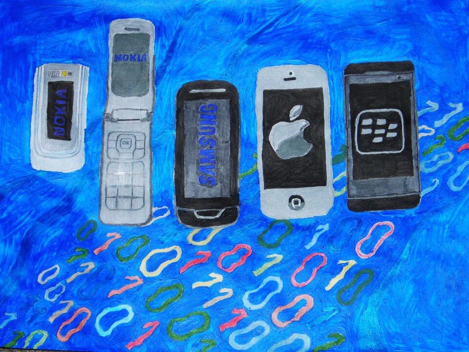
 Instead of duplicating Paul’s blog from last week, allow me to just show one of the slides Paul used to stimulate the panel discussion. It shows what a very basic phone (nicknamed “The brick” ), looked like 25 years ago. Its evolution to a very small high-performance communications- and computing device should remind all of us how miniaturization has changed this product and how rapidly it has divided our entire industry into successful vendors of smartphones and smartphone components and into companies who could not make the required changes fast enough.
The next wave of miniaturization has started already. Are you on board?
~ Herb
P.S.: After reporting about GIT2015 a week ago and about this “The Great Miniaturization” conference yesterday and today, allow me to give you a preview of December 2015 and invite you to the next multi-die IC conference I am contributing to:
The 12th 3D ASIP conference will be held in Redwood City (near SFO) from Tuesday, December 15 to Thursday, December 17.
My part, the 3D IC Design Tutorial, I’ll moderate on Tuesday afternoon, December 15, from 1 pm to 5.30.
In addition to a series of in-depth presentations from Interposer- and FOWLP design- and tools experts you’ll get, at no extra charge, a 250-page document describing the capabilities and plans of many 3D IC ecosystem players.


