Within the photolithography equipment market reaching US$ 150M 2014 (Source: Photolithography Equipment & Materials for Advanced Packaging, MEMS and LED Applications report, June 2015), advanced packaging applications have the strongest growth. Yole Développement (Yole) estimates that more than 40 systems have been installed in 2014, with a compound annual growth rate (CAGR) representing 10% between 2014 and 2020. In the meanwhile, MEMS photolithography equipment looks set for 7% CAGR and LEDs 3%.
Last June, Yole released its technology & market analysis dedicated to the manufacturing process, photolithography. Under this analysis entitled “Photolithography Equipment & Materials for Advanced Packaging, MEMS and LED Applications”, the “More than Moore” market research and strategy consulting company proposes a comprehensive overview of the equipment and materials market dedicated to the photolithography step. Yole’s analysts performed a special focus on the advanced packaging area. They highlighted the following topics: current and emerging lithography technologies, technical specifications, challenges and technology trends, market forecast between 2014 and 2020, market shares and some case studies …
“The advanced packaging market is very interesting and is growing dynamically as it includes many different players along the supply chain,” comments Claire Troadec, Technology & Market Analyst at Yole. It encompasses outsourced assembly at test firms (OSATs), integrated manufacturers (IDMs), MEMS foundries and mid-stage foundries.
In comparison, even if the MEMS & Sensors industry is growing at a fast pace, components are also experiencing die size reduction due to strong cost pressure in the consumer market. Consequently wafer shipments are not following the same trend as unit shipments. Lastly, LED equipment growth is back to a normal rhythm, after big investments made in recent years.
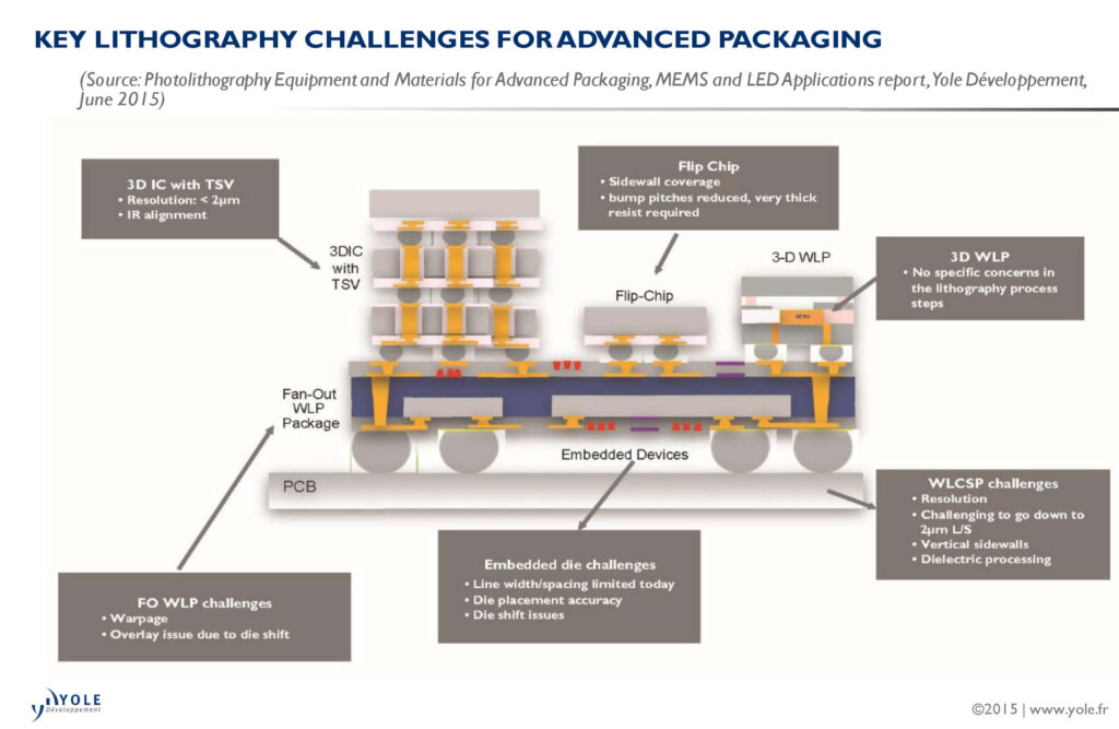
Advanced packaging has very complex technical specifications. Warpage handling as well as heterogeneous materials represent big challenges to photolithography. Due to aggressive resolution targets in advanced packaging, performance must be improved. The current minimum resolution required is below 5µm for some advanced packaging platforms, like 3D integrated circuits, 2.5D interposers, and wafer level chip scale packaging (WLCSP). A lot of effort is being made to reduce overlay issues due to shifting dies and obtain vertical sidewalls for flip-chip and WLCSP. Although steppers are already well established in the packaging field, new disruptive lithography technologies are also emerging and could contribute to market growth from 2015-2016.
“Huge business opportunities in the advanced packaging market are therefore driving photolithography equipment demand”, highlight Amandine Pizzagalli, Technology & Market Analyst at Yole. “Given the high growth rate of this market, there is no doubt that already established photolithography players and new entrants will be attracted”, she adds.
A detailed description of this report is available on i-micronews.com, manufacturing section.
Source: www.yole.fr


