
Yole Développement invites you to discover the main technology trends and business opportunities for 3D integration in 2015. As a research market & strategy consulting company, Yole Développement (Yole) works with the leaders of the advanced packaging industry every day to understand technical challenges and market issues. In this article, Yole’s analysts detail their vision of the industry, extracted from the technology & market analysis, 3DIC & 2.5D TSV Interconnect for Advanced Packaging 2014 Business Update.
3D integration has been in volume production for more than eight years for MEMS and CMOS image sensor products. 2006 was the year for the adoption of through-silicon vias (TSVs) in volume manufacturing, but not in the mainstream semiconductor business, which is focused on memory and logic devices. Today, the need for higher performance products – with or without cost constraints – is clearly driving broader adoption of 3D integration. Small volume field-programmable gate arrays (FPGAs) are now being followed by high-end memory and processor applications that use TSVs in volume manufacturing.
2015 will be the year that memory makers, mainly Hynix, Micron, Samsung and Tezzaron, enter the market with 3D stacked dynamic RAM (DRAM) for high-end applications. The importance of this move cannot be underestimated. 3D stacked memories have already been in sampling mode for two years and now the commercialization phase is finally starting.
In addition, Intel has announced the introduction of the first processor using TSVs with Micron’s Hybrid Memory Cube (HMC) stacked DRAM. This is the first big news of 2015, and AMD will certainly follow. Here also high-end applications are targeted, using 3D TSV integration to provide higher bandwidth memory and high-speed module capabilities.
The problem for wider adoption of TSVs in consumer electronic products is clearly the cost of manufacturing. TSV processes are not cheap, while the ‘Package-on-Package’ (PoP) platforms have been able to provide ever higher performance, better form factors, and lower cost. Yole therefore doesn’t foresee TSV technology pushing out PoP for lower end mobile applications in the next 3 years. Graphic applications could be the next target, but not before 2016.
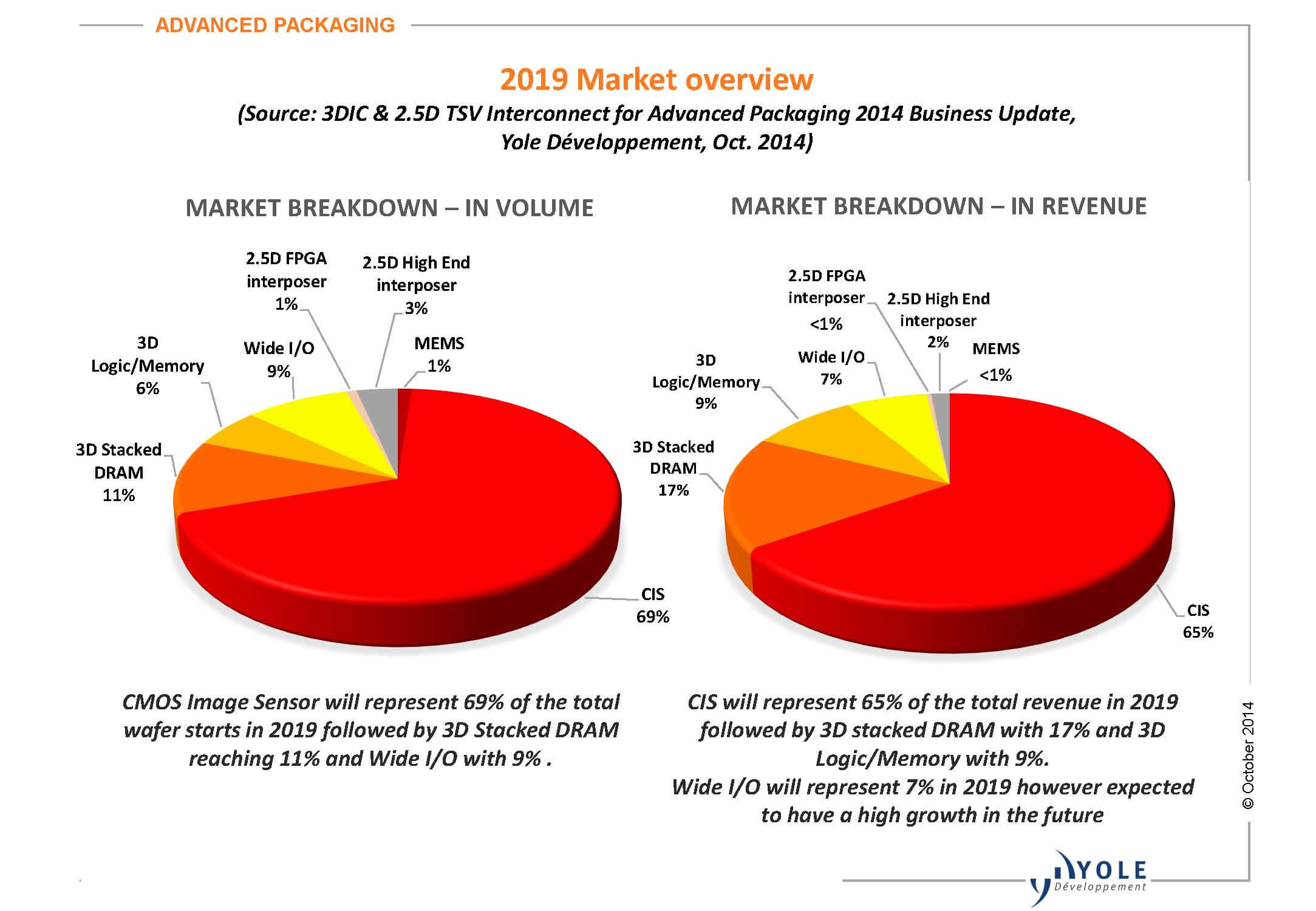
So what developments are needed to decrease 3D stacked devices’ manufacturing cost? The answer is very simple: make choices that decrease all material and equipment costs. Advanced substrates on organic materials or glass have to replace silicon interposers that are too expensive for middle- and low-end applications. Expensive process steps must be avoided in order to use existing equipment. But that will all take years, leaving MEMS and image sensors as still the key devices for TSV integration in high-volume manufacturing.

Other major changes will happen this year. Panel scale processing will finally go into volume production, using the Fan Out platform. Production platforms are expected to start moving from 300mm to 330mm wafer diameters and then rapidly to panel processing, paving the way for major changes in the supply chain infrastructure. This may be the next big change for 2015. ~ Jean-Christophe Eloy, President & CEO, Yole Développement