
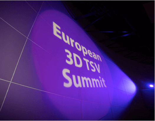
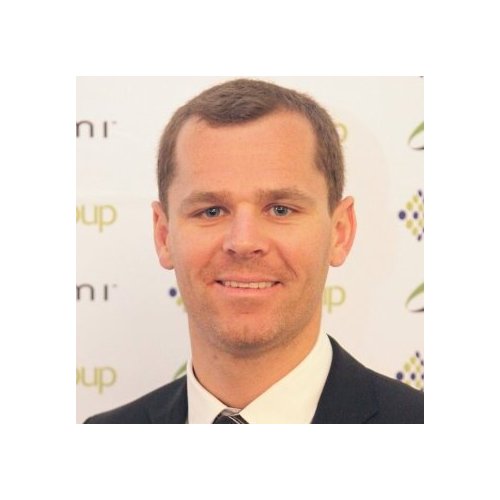
 In this Q&A interview with 3D InCites, Yann Guillou, Business Development Manager at SEMI Europe and the organizer of the European 3D TSV Summit since its creation, reminisces about his experience with the 3D TSV development over the years. He also talks about what inspired him to create the European 3D TSV Summit, the history of the Summit, and what the motivations are this year for the topic, Enabling Smarter Systems.
What do you think of the evolution of 3D TSV development in the last years?
3D TSV started to pop up as hot topic back in the years 2007-2008. After 2008, interest in TSV grew rapidly as more and more companies started to look at this technology and tried to understand what benefits it could bring to their products, what basic technology was necessary to successfully engineer products using TSV, the technology process flows and the business-related challenges. I was lucky at that time to be fully immersed in these analyses in the largest top European IDM, STMicroelectronics. With industry peers, and even with industry competitors, we were all learning from each other about the advantages and disadvantages of making different types of vias, about what dimension of key parameters could be defined, what type of stacking scheme made the most sense, about which type of companies were the most equipped to make these vias, and about how to carry out the backside processing or the stacking up to the final assembly, etc… I have to laugh a bit when I think back on all of the “crazy” ideas we were throwing around back then – laser via drilling, wafer-to-wafer stacking, very large via middle, or ultra-thin die some teams were trying to develop, and of course the initial cost targets we all had in mind at that time. Of course, we can now understand that most of these ideas were completely unrealistic, but at the time we took this research very seriously. Luckily, the industry has matured a lot since that time, and despite the fact that industrialization in high volume is taking more time than initially planned, experts are confident that 2015 will be a turning-point for wide-scale 3D TSV manufacturing.
This year’s conference topic is Enabling Smarter Systems – what was the main motivation for this?
 Each year, we try to have our conference theme reflect the current state of 3D technology as expressed by industry leaders. When SEMI created the European 3D TSV Summit in Jan 2013, we worked with the Summit’s steering committee, which is composed of leading European companies, to select the motto “On the Road Towards Manufacturing”. Our goal that year was to really delve into the “nitty-gritty” of the supply chain challenges being experienced by certain companies and to present the solutions that were being proposed by other companies. At the time, we were one of the very few events discussing what was missing in the manufacturing process of TSV products in high volume – “high volume” being, of course, subjective depending on the type of product and the industry you are targeting. We addressed items such as CoO and the major obstacles that could slow down the wide adoption of this technology, cost being identified as a major roadblock. The year after, in Jan 2014, industrial players were working hard to implement TSV manufacturing capability and capacity and we were not far for many product announcements that would integrate this technology. Thus for the 2014 edition, we chose the theme “Application Ready”. Some companies such as Amkor claimed that from a technological perspective, they were indeed Application Ready.
When we look at the most recent evolution of 3D TSV technology, we see that TSVs have become an indispensable part of the smarter systems development, so the theme “Enabling Smarter Systems” seemed to stem quite naturally from this. In essence, to have commercial success, products need to be developed in an intelligent way, from the architecture, design, process, packaging, and test. TSV technology begins to stand out as one of THE key enablers of this smart Integration. Whether we’re talking about high performance computing, memories, CMOS image sensors or MEMS, TSVs allow engineers to provide better integration, to improve system performances, and in some specific cases, an approach with TSV can even demonstrate cost benefits at a system level compared to more traditional solutions. Obviously, as with any new technology, the technology is not 100% satisfying yet and, given more time, development teams will continue to have a better and better grasp on the underlying benefits of TSV. Still, with more and more smart systems using TSV being manufactured, my feeling is that industry is on the right track.
How did you select the keynote speakers?
SEMI stands for Semiconductor Equipment and Materials International. Even if our member base is not limited to Equipment and Materials (E&M) companies and includes organizations from the entire supply chain, E&M companies still represent a large portion. What these members want hear is the voice of their customers, or their customer’s customers. Consequently, for keynote talks, we try to target these types of customer companies, which include IDMs, OSATs, fabless, or end-user device makers. Of course, we are always looking for leading and influential companies for such type of presentations and we hope that they will share their latest perspective with the audience.
Looking at the 3 keynotes talks we recently announced, we are excited with what we’ve been able to propose to attendees for this next edition. Having Microsoft and their Smart Devices Group ready to share with us the trends they’ve identified for 3D IC and how it might impact their product portfolio is unique. For years, Timo Hentonnen, the speaker of Microsoft, has been a key person at Nokia in the packaging group driving new technology developments and implementing them in large volumes. Now, with Nokia’s mobile phone unit having been absorbed into Microsoft, what Timo will share with attendees should be a highlight of the Summit.
We are particularly excited to have Bryan Black with us this year. He is a senior fellow at AMD. Bryan will take advantage of his keynote speaking role at the European 3D TSV Summit to present attendees with new important information about AMD’s activity. As you know, AMD has been working closely with memory partners to develop a disruptive product that would solve the bandwidth crisis. Let’s wait a few weeks and we will see what he will present. I’m convinced it will be a major announcement.
Last, but certainly not the least, we are honored to propose a talk from the world’s leading OSAT, ASE. Bill Chen, fellow and technical advisor, will be joining us for a keynote presentation. Bill rarely delivers talks in Europe, and I’m sure he will have key messages to pass on to attendees in his explanation of how ASE sees TSV contributing to their upcoming business activities.
What was the motivation behind dedicating the pre-conference symposium to a Market Briefing?

Every activity or event we organize is based on a current business activity or potential business activity of our members. SEMI is a trade association and one of our main goals is to inform and support our members in detecting business opportunities. Having dedicated presentations on the market is not new to the 3D TSV Summit; this has been the case since the creation of the European 3D TSV Summit. However, this year, we decided to emphasize this aspect, following the evolution of the growing 3D IC market. As I said earlier, 2015 is projected to be a game-changing year for 3D TSV, with memory companies beginning to manufacture high end products. We invited some of the most trusted experts in the domain including AlixPartners, ATREG, TechSearch International and Yole Développement, to share their latest updates. Presentations by Yole and Teachsearch International should be particularly interesting, as both companies recently released updated reports on 3D IC with the latest key statistics on the market potential of 3D TSV technology. AlixPartners and ATREG do not frequently speak on the topic of 3D TSV, so attendees will have a special opportunity to hear fresh information on the market from these two speakers.
The agenda appears to be broad and touch on many topics. What was the committee’s criteria for setting the agenda?
As full program demonstrates, the European 3D TSV Summit features 60% international speakers. Since its inception, the European 3D TSV Summit has been a global event. Despite the location being in Europe, we have succeeded in making the Summit a truly International Forum for any and everyone involved 3D TSV, regardless of country of origin. This is why we have insisted on building an agenda that represents global and not only European interests.
Secondly, in a continued attempt to deliver our attendees with fresh and industry-relevant conference content, we adopted a few topics this year that were not necessarily addressed in prior years, but appeared to be particularly relevant to us. For instance, we wanted to have some presentations on “Interposers”, from a product and business perspective as well as from a technology perspective. In this regard, on the interposer technology side, we will take a closer look at the glass approach that is important not to neglect. Another example is a focus on Photonics and how TSV can enable smarter integration in the future for this type of application. For this last session, we have invited IBM and HP, who are both looking at developing TSV technology in photonics.
Finally, we always try to propose new companies and speakers to reflect the countless diverse viewpoints and experiences in the industry. For instance, I’m curious to attend Qualcomm and KLA-Tencor’s presentations and listen to what they will share with the audience.
What is unique in the experience you are proposing to attendees?
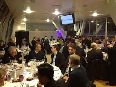 To steal your word, I would say that we are proposing a full “experience” for attendees and not “just another conference”. At least, this has been our hope and intention since we created this event. The event is a unique combination of keynote and invited talks, industry-relevant panel discussion and a quite specialized exhibition that receives high foot traffic. On top of that, we offer high-quality networking during lunches and during the gala dinner, as well as possibility to schedule one-on-one business meetings between attendees during the event. As in the past years, we expect that this year there will be more than 40 hours of cumulated one-one one meetings. Finally, the event will be hosted by Minatec, a venue that shares the CEA-Leti campus. From the windows of the exhibition you can see the clean rooms where 300mm wafers are processed from via etching up to stacking. I’m convinced that this high-tech environment stimulates the interaction between people. We discuss TSV in a location where TSV are made! This also opens the possibility for the Summit to offer, as a side activity, a visit to the TSV line of CEA-Leti for up to 50 people.
Visit the 2015 European 3D TSV Summit website for more information and to register.


