


I don’t usually write about MEMS. But every once in a while, when MEMS (stands for micro-electromechanical systems) touches anything to do with 3D integration, usually at the system-level, I might veer slightly out of my comfort zone to interview a MEMS supplier about their latest developments. I find it’s a good way to learn about the synergies and to cross-pollinate information. Today was one of those days. I interviewed Steve Breit, PhD, VP of Engineering, Coventor, supplier of design automation software for MEMS and semiconductor applications. Breit reminded me that through silicon via technology (TSV), which is critical for 3D IC, owes a debt to MEMS. He’s right about that. So I figure a nod to MEMS now and again on 3D InCites isn’t out of place.
Breit briefed me on the company’s latest version of its MEMS+ modeling environment for accelerated development of advanced MEMS devices and systems, and what the improvements mean for ASIC designers who need to integrate MEMS devices into their system design.
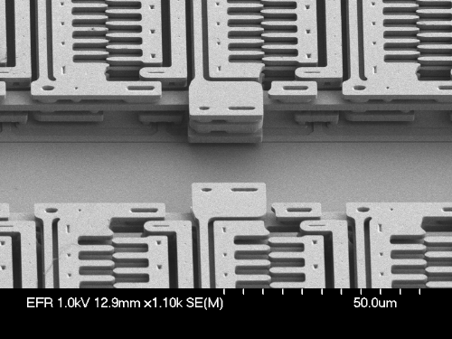
MEMS + is a tool for creating high order finite element models that run in MATLAB, Simulink, and Cadence instead of proprietary field solvers (Figure 1). Where this tool applies to the 3D integration space is for wafer bonding and wafer level packaging, explained Breit. Up until recently the industry has integrated MEMS and CMOS devices using monolithic processes or side-by-side on separate dies. However as CMOS advances and MEMS take up more real estate, that is changing and the industry is turning to a 3D stacking approach. “We’re seeing fewer monolithic and side-by-side solutions and more cases of flipping the MEMS wafer, bonding it to the ASIC and dicing it up. The ASIC wafer then provides some of the package.” What this means is, the ASIC system designer needs to integrate MEMS models into their designs, and this is where MEMS+ 5.0 comes in.
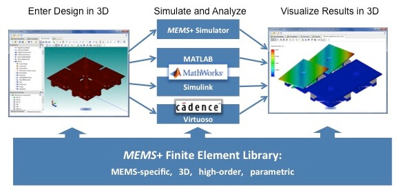
Traditionally, MEMS and ASICs are designed in their own silos. Currently, getting a MEMS model into and ASIC design is performed manually, which is inaccurate, error prone and requires additional “build and test” cycles for integration. In the previous iteration of MEMS+, a MEMS model can be auto-generated and inserted into a companion ASIC design tool such as MathWorks MATLAB® Simulink® or Cadence Virtuoso. But there were so many degrees of freedom that the simulation process was too slow to meet the ASIC design requirements. The 5.0 version includes a new capability to create and export reduced-order models (ROMs), which have fewer degrees of freedom, to Verilog-A format and to the MATLAB Simulink environment, to enable extremely fast and accurate non-linear simulations of MEMS-based systems. It’s the ROM addition that makes this tool not only attractive to MEMS designers but also appealing to ASICs designers because it meets their simulation speed requirements.
MEMS+ is part of Coventor’s simulation tool platform, which also includes the CoventorWare® and SEMulator3D® suites. According to Breit, it’s the third tool on this list that can be used not only for modeling MEMS processes, but also applies to the semiconductor space, specifically for advanced 3D transistor structures (FinFETS) and complex memory structures like 3D NAND. “There were no tools for the semiconductor process integration flow from the front-end to the back-end, where you’re putting together processes that have hundreds of steps,” explained Breit. “Semulator 3D supports that. Process engineers are using it to model finFETS and 3D memory.”

Is a simulation tool for die stacking on Coventor’s roadmap? “Since our specialty is detailed geometry, our tools are more suited to on-chip 3D structures rather than chip-to-chip architectures,” said Breit.”However there is potential use for developing TSV technology down the road in some capacity, if it becomes critical for modeling every TSV on the die or wafer as densities become tighter and TSVs scale down.”
For more information on Coventor, be sure to follow their blog. ~ F.v.T.


