
Is Si photonics the vehicle that will finally catapult 2.5D and 3D IC to stardom? While that was the story told during an R&D panel at SEMICON West, it’s not exactly accurate. At this week’s 3D Architectures for Semiconductor Integration and Packaging (3D ASIP) which took place Wednesday, December 11, 2013 at the Hyatt Regency San Francisco Airport, it became clear that High Bandwidth Memory (HBM) is more likely to be the application that brings 3D TSVs to volume manufacturing. However, according to Dim-Lee Kwong, executive director of IME in Singapore, Si Photonics holds the key for integration of memory and logic, and enables wafer level integration of multiple components. Individually, While Si photonics and through silicon interposers (TSI) each provide advantages over scaling and monolithic SoCs, Kwong says together they can move “Moore’s Mountain” as we approach CMOS scaling limits.
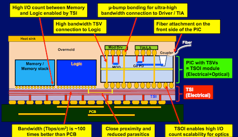
“Si photonics bring the economics of CMOS electronics to photonics,” said Kwong. “We can replicate the semiconductor fabless model for photonics and allow designers to design innovative products, all the way to packaging and test.” Further, he said Si photonics combined with a through silicon interposer (TSI) can solve the issues of degraded system performance and increased power consumption at data centers caused by increased internet traffic (Figure 1).
Kwong was among the speakers featured during the pre-conference symposium, Si Photonics, Coming of Age, at this year’s 3D Architectures for Semiconductor Integration and Packaging (3DASIP). He offered the R&D perspective, sharing IME’s activities in integrating Si Photonics on a TSI platform. Also among the speakers was Stephane Lessard, Senior Specialist, Photonics System Architecture, Ericsson Research, who offered the vendor’s perspective of integrating Si photonics with memory and logic, the performance advantages that can be achieved, and the growing need to address the data explosion that can’t be solved with Cu technologies.
IME has developed two key technology platforms necessary for lower power, high bandwidth interconnect. One involves CMOS compatibility with Si Photonics for short-reach interconnects, and the other is low-cost 2.5D TSI for heterogenous integration of Si photonics and advanced electronics to achieve high performance, high-density interconnects. “Heterogeneous integration of Photonics with optical transceiver, logic, and memory is the way to go rather than SOC.” said Kwong.
Kwong reports that memory and logic are ready, and a 40G Si photonics platform has been developed. The challenge lies in the packaging of Si photonics chips. “60-70% of cost for Si photonics is the packaging; there is no semiconductor way to do it.” he noted. The main issue is with achieving low-loss optical coupling. He explained that the light signal has to come into the package via fiber optics, and then needs to be converted to an electrical signal inside the package, and then be converted back to a light signal upon leaving the package. Kwong expects IME will have worked out the issues in the next 18 months. “TSI provides a nice platform for interconnecting photonic ICs (PIC), logic, Memory and CMOS as close as possible on the interposer.” said Kwong.
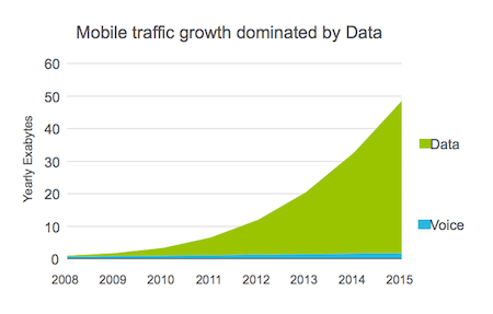
Stephane Lessard echoed Kwong on the need for Si Photonics to address the data explosion. He predicted that LTE will cover 60% of the world’s population by 2018, and we’ll be dealing with transmitting 12x the data as what we have now. This will impact routers, microwave backhaul, and radio base stations. “The power requirements are huge,” he said, adding that keeping everything in Cu will result in power consumption and cooling issues. “We need to 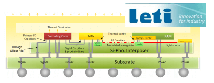 rethink systems and lower power consumption.” Cost structure is also a challenge, because consumers expect to pay the same for LTE as they do for 3G. Copper is at an inflection point, he noted, and said replacing electrical pathways with photonics is a good solution, because Si photonics can help solve the space, miniaturization and density issues, additionally it adds flexibility you can’t get from monolithic systems. The solution lies in the packaging because Si photonics can fully benefits from electrical 2.5D and 3D ecosystem, and “blends right in.”

Lessard said that a key weapon is the optical engine that performs electrical to optical conversion, but that it only solves part of the problem. He also agreed with Kwong’s assessment that what’s missing is a “solid story about optical coupling” of silicon and volume packaging. One conclusion Ericsson came to awhile ago, is that the electrical signals need to stay local to the processing unit as long as possible, but when the signal needs to get out of the package, it should be done optically.
“This is craftmanship and has to be normalized in the next 2-3 years when we’re going to need it.” he added that the long-term vision for Si photonics and packaging is to se Si photonics commoditized. He also said that the lack of ecosystem readiness will cause problems for data communication and traffic. “People will be running to find places to put equipment.” What’s the timeframe for this? Lessard said 2016-17 would be a nice time for all these things to come into play. “If you have something working by this time, I guarantee you will not go bankrupt,” he said.
“Photonics does give you more.” he said. “Once you’re rid of electrical batteries and use signal on an optical layer, there’s a whole lot of things you can dream of. Putting Si photonics and packaging around the same table is essential. Lets go for it and lets solve the problem. 2;5 and 3D are definitely way to go.” ~ F.v.T.


