
I listened in on yesterday’s webcast, 3D and 2.5D Integration: A Status Report Live Event hosted by Solid State Technology, and while most of the information was similar to what I had heard at IMAPS Device Packaging Conference, EDPS, ECTC 2012, etc., they are clearly messages worth repeating, and some new interesting nuggets as well.
Jan Vardaman, from TechSearch International, started things off with an overview of the markets for 2.5D and 3D TSV, assuring listeners that “There’s no doubt 3D TSVs are going to happen at some time….. people are looking at the cost compared to alternatives, vs. the performance gains they’ll get.” However, she says that every time she sees a company’s roadmap, the dates for 3D IC adoption shifts further out. She illustrated that with an older roadmap from Renesas, which shows an ultrathin, ultracompact TSV package hitting the market in 2011 (which as we all know by now, never happened.)
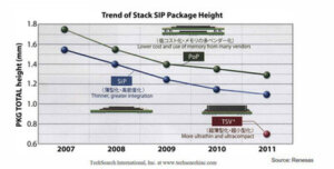 Courtesy of TechSearch International
Why does this keep happening? Vardaman cites a couple key issues. First, is a lack of thermally-aware design tools. “Thermal issues are a killer” especially when stacking DRAM on logic. She said she’s not aware of any such tools that are commercially available yet. Second was the debond step in the temporary bond/debond processes. “The debond step has to have very high yield and we’re not there with that yet,” Although materials companies continue to work on solutions. She pointed to Dow Corning’s recent announcement as an example. Third and one of the most critical is Test. “We need to talk about test a whole lot more” and this includes known good die (KGD) known good substrates (KGS), methodologies for test, probe cards, will we probe, and reliability data needs to be available to the end user. Vardaman also said that the assembly process and infrastructure logistics must be resolved.
Lot of applications are turning to 2.5D with interposers in the interim. Techsearch predicts the adoption of TSV interposer will happen before true 3D IC. (Not earth shattering news). But Vardaman shared a preview of market numbers to be released in July, and compared to past forecasts, shows the full TSV stack shifting out
 Courtesy of TechSearch International
Dave McCann of GlobalFoundries and Bill Chen of ASE, followed Vardaman, each focusing on the importance of collaboration in the supply chain, representing the foundry and the OSATS, respectively. Much of what they presented were similar to the messages presented at ECTC in Greg Bartlett’s keynote and by Chen during Packaging Foundry Panel.
McCann talked about one of my favorite topics: scaling vs. packaging solutions to achieve power and bandwidth performance. He said they continually hear from customers, “I want to keep scaling, but I need to have a performance advantage with that scaling.” McCann says the issue is no longer the performance of the individual chip, but the access to memory that is critical. Memory scaling is not keeping pace with digital scaling, regardless of the market (mobile, server, PC). McCann also talked about how the cost of running a data center is non-hardware related, but has more to do with power consumption. We need to find a power solution that lowers the cost. “In the past, the answer was to integrate more and more on one IC, but the number of mask layers needed to achieve this is exploding,” noted McCann. Overall lithography cost is going up while benefits of scaling are being reduced. “In order to generate performance or go to the next digital node, we must solve the memory bandwidth issue to reduce overall power.”
And its 2.5D and 3D to the rescue! McCann designated the target applications for each succinctly, and also said 2.5D is a long term, rather than interim answer. 2.5D is the memory bandwidth solution for high power applications, while 3D IC stacking is the solution for low power memory bandwidth applications. He also provided an adoption roadmap, shown below.
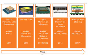 ≈Courtesy of GlobalFoundries
Both McCann and Chen talked about the changing supply chain models, supporting collaborative efforts. McCann said the IDM model is not the way to go for two main reasons: it provides a single solution and promotes a slower rate of change. Open collaboration allows for flexible solutions that come to market more rapidly. Another advantage of open collaboration is the transparency it provides to customers, which they will need to commit to new technologies. At the end of the day, McCann says the success will be determined by yield (which ultimately defines the cost.)
Chen called his collaborative model a Virtual IDM that comprises chip architecture and design, semiconductor manufacturing, and he presented a thorough history of the transition from wire bond, to flip chip and wafer-level packaging, which has lead us to the 2.5D and 3D technologies we have today.

The final speaker of the webcast was Brent Przybus, Director of FPGA product line marketing, Xilinx, offered the end-user perspective. Everyone is very familiar with Xilinx’ Virtex 7 FPGA, touted as the first 2.5D product on the market. Xilinx also recently introduced it first heterogeneous 3D version of the product, Virtex-7 H580T FPGA, which comprises 2X FPGA dice and 1X 8-channel 28Gbps transceiver die in the same package. Pryzbus reported the company has shipped Virtex-7 20001 in the thousands, and H580T in the hundreds.
From Xilinx’ perspective, what 3D buys is connectivity. I/O bottlenecks are removed because you now have connections from within the device. No longer limited by I/O constraints means increased capacity, which in turn allows for the exploration of “crossovers” combining logic, memory, analog, etc.
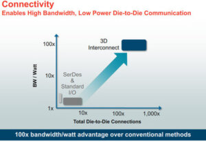 Courtesy of Xilinx
With regard to addressing 3DIC challenges, Przybus shared some of Xilinx’ experience. He said it’s important to consider the mechanical and thermal domains as well as the electrical domain in the architecture. He advised to put the high performance (hot) chip on top for thermal and TSV process availability. Its also important to maximize, understand and model the keep-out zone (KOZ) around the TSVs properly to build a system to its greatest capacity, and that means good floorplanning is needed.
Przybus’ call to action includes design enablement in terms of EDA tools (Xilinx built some of their models themselves with what ws available) as well as Process Development Kits (PDKs) for manufacturing. Design for test is important, and standards are critical, particularly in the area of design rules for TSVs, microbumps and the KOZ; TSV and microbump materials, and thermal budget.
So to recap – overall, the sticking points are still in design, test, standards, and the supply chain infrastructure, although progress on all counts is definitely being done.
The word for the day? COLLABORATION. Hands down, the best comment of the whole webcast came from Bill Chen, speaking to Mark Bohr’s now famous declaration that the “fabless model is collapsing.” Chen quoted Charles Darwin, “In the long history of humankind, those who learn to collaborate and improvise most effectively have prevailed.” Amen!


