
The 3D NAND floodgates just opened a little wider with today’s announcement from BeSang that it has developed 3D Super-NAND technology, based on a monolithic 3D IC process, True 3D™ IC, claiming to be the “lowest cost-per-bit in the NAND market.”
With all the recent 3D NAND discussion and announcements about Samsung, Toshiba, and Intel and Micron’s 3D X-point, I wanted to know more. Specifically, what makes BeSang’s 3D Super NAND different from the others? Sang-Yun Lee, CEO, BeSang, was more than happy to comply.
The last time we spoke was a few years ago, when the Beaverton, OR-based fabless semiconductor company announced it had licensed its True 3D™ IC, to SK Hynix, intended for use across a range of products including DRAM. So I started out by asking for an update on that announcement.
Lee explained that while 3D DRAM using the True 3D IC process has been tested and verified at 30nm feature sizes, it has not yet been commercialized. “BeSang does not develop 3D DRAM by itself, it just licenses the 3D DRAM technology and is therefore not able to share details,” explained Lee. “However, BeSang will be the product company for the 3D super-NAND.” He added that while 3D DRAM and 3D super-NAND look similar and share the same platform technology, True 3D IC, they have different types of charge storage.
Why go 3D with NAND?
Lee explained that planar NAND faces lateral scaling (i.e. Moore’s Law) limitations due to large leakage current and less gate-controlled charges. Therefore, 3D NAND seems to be the inevitable choice for increasing memory density in a given silicon area through vertical stacking. However, it’s not that simple. Because as always in the semiconductor world, cost is king, and the customers are the ones who decide when it’s time to take the plunge.
For example, Lee says that although Samsung initially declared 16nm to be the end of planar NAND, and invested >$10B in 3D NAND, it has also begun development of 14nm planar NAND. He said that according to the Digital Daily in Korea, (and as I don’t read Korean, I’ll take his word for it.) fab utilization of Samsung’s 3D NAND fab is less than 50% due to the delay of product qualification from customers.
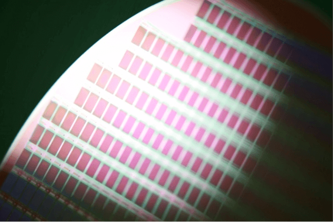
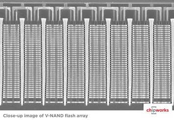
“It is well-known that 3D NAND still has yield and reliability issues due to extreme process complexity,” said Lee. “If we see the image of stacked cell layer only in the 3D NAND, it looks amazing. (Figure 1) However, if we consider the whole 3D NAND picture, we begin to understand the issues.” (Figure 2)
The 3D NAND Cost Conundrum
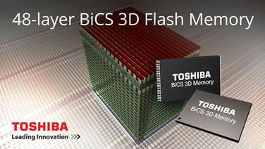
“Memory companies have announced 3D NAND with memory capacity of 256Gb or more, with up to 48 stacked layers,” noted Lee. “While this is certainly good news for high memory capacity, the most important factor in memory is Cost-per-Bit.” He said according to Mark Webb, MKW Ventures, who spoke at the 2015 Flash Memory Summit, 32-layer 3D NAND cost is currently 70% more expensive than planar NAND at full production.
What makes it so Costly?
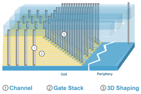
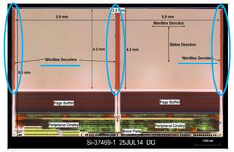
Lee explained that 3D NAND has large and complex staircase contacts areas, as well as large page buffers and periphery logic areas. In general it takes more than 10 weeks to process stacked memory cells, staircase contact, and periphery logic areas sequentially. (Figure 2a and 2b)
Long wafer processing time causes low throughput and high ‘Cost-per-Bit’. A huge investment is needed to increase throughput. Can 3D NAND justify ROI from the huge investment? “No one knows the answer at this moment,” says Lee. “However, it is certain that it will take a long time.”
Another cost component to 3D NAND is its reliance on lithography processes. 3D NAND requires high aspect ratio holes to implement vertically oriented flash memory cell array (Figure 3). Lee says it’s a misconception that 3D NAND manufacturing reduces the dependence on expensive lithography processes. Samsung, for example, is using 40nm feature sizes for the hole. As number of stacked layers increases, it becomes more difficult to reduce the hole feature size because aspect ratio of hole increases. “3D NAND cannot avoid expensive lithography processing in order to reduce feature size in other areas,” explained Lee. “3D NAND has later scaling limitations due to the high aspect ratio of holes, and still relies on expensive lithography processing.”

Comparison of 3D NAND and 3D Super-NAND
According to Lee, BeSang’s 3D super-NAND is based on BeSang’s TRUE 3D IC, which implements memory cell arrays on top of logic. In this comparison, 1-layer 3D super-NAND (i.e. only 1-layer memory cell layer is added on top of memory logic) is compared with 48-layer 3D NAND because even 1-layer 3D super-NAND could have better ‘cost-per-bit’ compared to 48-layer 3D NAND. (Figure 2)
While 3D super-NAND requires advanced feature size (i.e. 10nm) for cell formation to achieve high cell density, it takes only five mask steps and five days of processing time, noted Lee. So, 3D super-NAND could achieve high throughput with limited dependence on expensive lithography processing. In parallel, memory logic wafer can be manufactured at an old generation fab using affordable lithography processing. Here is the comparison:
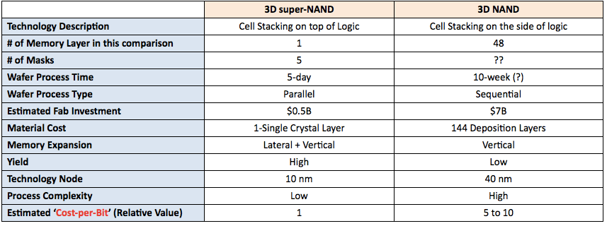
How is it possible to reduce the processing time from 10 weeks to five days? Lee credits “the noble integration of monolithic 3D IC.” And because the wafer processing time is so short, he says a fab could generate high-throughput manufacturing of 3D super-NAND with just $0.5B investment.
Lee explained that the cell formation of 3D super-NAND utilizes vertical silicon nanowire with Surround Gate Transistors (SGT). Therefore, there is no concern about leakage current and gate controlled charge. He says it has been proven that silicon nanowire works well as a flash memory as small as 2nm.
Unlike 3D NAND, 3D super-NAND does not have high aspect ratio holes. So, it is relatively easy to scale in lateral dimension. Also, if more memory is needed, more layers can be added vertically.
Considering cell density, number of cell layers, cell efficiency and throughput, Lee estimates that 1-layer 3D super-NAND has 5 to 10 times better ‘Cost-per-Bit’ compared to 3D NAND. “If 3D NAND wants double its memory capacity, then 48-layers becomes 96-layers,” explained Lee. “However, 1-layer 3D super-NAND only needs to add one more memory layer to make its memory capacity double.”
BeSang’s Challenge
While BeSang’s wafer processing is fairly simple, because it requires 10nm feature sizes, finding a manufacturing partner is a bit of a challenge. There aren’t many options, says Lee. However, he says BeSang is in discussions with potential partner companies, and once that is ironed out, ramping to production will be fast and easy. Lee expects 3D Super NAND could be on the market as early as the end of 2016. The first target product is 128Gb NAND with 1-layer 3D super-NAND. ~ F.v.T.


Comments are closed.