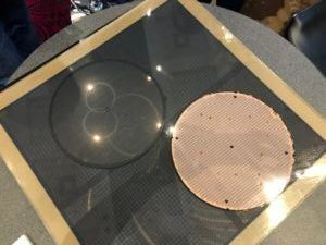
Deca Technologies is pleased to announce that it has reached an agreement with nepes Corporation (nepes) whereby nepes will expand its geographic footprint and manufacturing capabilities by taking over the operations of Deca Technologies’ Philippines manufacturing facility. The investment will permit the expansion of the WLCSP capacity already in mass production and will now offer up to 100,000 wafers per month, with a dual-site capability courtesy of the Korea site, in addition to the Philippines facility.
As part of the agreement, nepes has licensed Deca’s M-Series technology to further enable the rapid industry adoption of advanced fan-out technology. Deca’s revolutionary M-Series with Adaptive Patterning combined with nepes’ strong experience in fan-out and large-panel manufacturing creates a powerful combination for future growth.
Multiple industry research firms have identified M-Series designed into several tier-one handsets in support of a leader in PMIC applications. Further announcements are expected to follow as more customers adopt the technology. Integration of nepes’ large-panel and SIP capabilities with M-Series and Adaptive Patterning will create multiple exciting customer module solution possibilities including advanced heterogeneous integration.
“This is a very exciting time for Deca Technologies,” said Dennis Yost, CEO of Deca Technologies. “Our patented M-Series is becoming the de facto industry fan-out standard. We see multiple customers keen to rapidly grow their use of M-Series fan-out packaging. With nepes’ experience, this can only accelerate the technology’s adoption. Plus, the portfolio of technologies nepes can provide will supplement the range of offerings we can provide to our existing customer base to continue to expand our services to them.

“By this collaborative work, I believe there will be great synergy of M-Series technology with our panel-level packaging, enabling technology for customer future products and providing them strong differentiation,” said Jay Kim, SVP of Operations and Technology for nepes Corporation. “Our ability to now complement nepes’ existing capabilities of fan-out and large-panel package experience with M-Series technology, and offering this in two sites, will be a key part of our growth strategy moving forward, as well as expanding the services for existing customers and enabling us to become a top 10 semiconductor assembly services provider.”
About nepes
nepes Corporation (www.nepes.co.kr), founded in 1990, has been providing bumping and wafer-level package OSAT manufacturing services in partnership with fabless and IDM customers worldwide since 2001. nepes offers turnkey solutions of IC back-end service for 8″ and 12″ wafers with reliable quality by implementing mainstream technology from wafer bumping, IC packaging and testing. The company’s portfolio of products covers wafer-level package (WLP), fan-out wafer-level package (FOWLP), fan-out wafer-level system in package (FOWL-SiP) and panel-level package (PLP), which is a hybrid package manufacturing technology that has revolutionized the mass production experience of advanced semiconductor packaging with the touch-screen panel (TSP) production line for LCD. nepes has manufacturing sites in South Korea and China and international sales offices in San Diego, California and Shanghai, China.

Media Contact & Deca Technologies Company Contact:
Garry Pycroft Vice President of Sales & Marketing
garry.pycroft@decatechnologies.com
nepes Corporation Company Contact:
Jim Kim, Director of Sale
jimkim@nepes.co.kr
+82-10-6261-5940