

IIFTLE is always on the lookout for technologies that will require advanced packaging solutions. Fingerprint sensors for today’s latest smartphones appear to be one of those applications.
Packaging for Fingerprint Sensors
DIGITIMes recently reported that the manufacture of under-display optical fingerprint sensors for use in 5G-enabled phones will require extensive wafer-level backend services (i.e. advanced packaging. Their sources report that available under-display fingerprint sensors for standard smartphones are currently bonded to CMOS image sensors and assembled in one package at module assemblers instead of IC packagers that are responsible for most of the backend part, including the final testing. Optical fingerprint sensor suppliers such as Goodix (engaged in the supply chain of major China-based smartphones) and Egis Technology (supplying Samsung) have reportedly adopted the method also for cost reasons, placing packaging orders for their under-display solutions mainly with module assemblers.
However, when 5G becomes fully commercialized, chip packages will be required to be even thinner, which can be better achieved through wafer-level packaging which is available from most outsourced semiconductor assembly and test service (OSATS) providers. ASE is reportedly getting ready for this eventuality, while Xintec and VisEra Technologies are also readying for this market growth. Chip demand for 5G smartphones is set to expand starting in 2020.
Lets take a look at the technologies that are being used. Today fingerprint sensor technology exists in optical, capacitive, and more recently, ultrasonic variants.
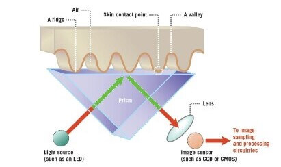
Optical Fingerprint Sensors
An optical fingerprint reader bounces light up to your finger and back down to the sensor, which interprets the reading as a 2D image. Essentially it takes a photograph of your finger to determine the pattern of ridges and valleys. This technique captures an optical image and detects patterns (ridges or unique marks) on the surface, by analyzing the light and dark regions of the image. Experts report that this approach is relatively easy to fool with a photo, a fingerprint transfer, or a prosthetic fingerprint.
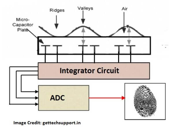
Capacitive Sensors
The most common fingerprint scanner in smartphones today is the capacitive scanner. Capacitive fingerprint scanners use arrays of capacitor circuits to collect data. Once captured, this digital data can be analyzed to look for distinctive and unique fingerprint attributes. This technology is much tougher to fool than an optical scanner since the results can’t be replicated with an image and is incredibly tough to fool with some sort of prosthetic, as different materials will record slightly different changes in charge at the capacitor. Security risks come from either hardware or software hacking.
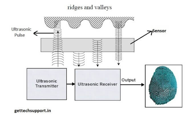
Ultrasonic Sensors
The latest fingerprint scanning technology to enter the smartphone space is the ultrasonic sensor. The hardware consists of both an ultrasonic transmitter and a receiver. An ultrasonic pulse is transmitted against the finger that is placed over the scanner. Some of this pulse is absorbed and some of it is bounced back to the sensor, depending upon the ridges, pores and other details that are unique to each fingerprint. A sensor that can detect mechanical stress is used to calculate the intensity of the returning ultrasonic pulse. Scanning for longer periods of time allows for additional depth data to be captured, resulting in a highly detailed 3D reproduction of the scanned fingerprint. The 3D nature of this capture technique makes it an even more secure alternative to capacitive scanners.
Ultrasonic scanners hides under the display, meaning that the waves have to travel through the display’s backplane, glass, and protective cover before reaching your finger. Qualcomm’s ultrasonic technology works through glass that’s up to 800 microns thick. It’ll capture your details through water, lotion and grease, at night or in bright daylight. Qualcomm also claims it’s faster and much more secure than the optical fingerprint sensor. But, it only works with select screen protector layers due to its thickness limitation.
Samsung’s latest Galaxy S10 and S10 Plus are the first phones to use Qualcomm’s ultrasonic in-screen fingerprint technology.
TSMC – “Moore’s Law Never was”
On a separate topic, Godfrey Cheng, Head of Global Marketing for TSMC has recently written an interesting blog on the TSMC web pages.

We all know Moore’s “Law”, simply states: The number of transistors in an integrated device essentially doubles about every 2 years. Also, as we all know, this has been physically achieved through the use of scaling technology. But, strictly speaking, as IFTLE has been stating for years, and as TSMC now similarly espouses, this has never been a “law”. A “law” is something like F=MA (force =mass x acceleration). Gordon Moore never called it a “law”, others mistakenly did. Certainly, his observations and predictions have largely held true for the past several decades, for which he deserves all the credit he has gotten, but it has never been a law so no laws are now being broken.
Cheng goes on to correctly state that “It would appear that some have conflated “Moore’s Law” to mean that the performance of a chip, given the same area, doubles every 2 years. For many years, particularly in the development of CPUs and GPUs, this appeared to hold true. From the 1970s to early 2000’s, there was an explosive increase of transistor clock speed going from single megahertz to multiple gigahertz, respectively. However, since the (early) 2000’s, compute performance has largely increased not through the improvement of the transistor clock speed but rather through both silicon architecture innovation and the threading or parallelization of computing workloads.”
Cheng continues “To feed modern fast CPUs, GPUs and dedicated AI processors, it is critical to provide memory that is both physically closer to the cores that are requesting the data for improved latency, in addition to supplying a higher bandwidth of data for the cores to process. When memory is collocated closer to the logic cores, the system achieves lower latency, lower power consumption and higher overall performance.”
The physical distance between memory and logic is what limits bandwidth and performance through increased latency. In addition, power consumption for logic and memory also govern a circuit’s performance, especially in portable applications such as smartphones or IOT devices. It is advanced packaging that brings memory closer, i.e a 10nm chip in a BGA package will not deliver the performance that is needed in today high end devices.
TSMC holds their position in the industry today partially because they were early to recognize that Advanced Packaging would be instrumental in the integration of logic cores with memory. As detailed in past IFTLE, TSMC has pioneered advanced packaging techniques that deliver a complete system with a silicon-based interposer or fan-out-based chiplet integration. They also have developed advanced packaging techniques that allow them to stack chips on wafers or stack wafer on wafer prior to integration into packaged modules. These advanced packaging techniques allow TSMC customers to deliver much higher density and more performance than most of their rivals.
For all the latest in Advanced Packaging stay linked to IFTLE……………………


