
If you drive a late model car, you may be impressed by the many sensors that capture engine conditions, tire pressure, etc. and report to you. Many cars even call the factory if they need preventive maintenance. Wouldn’t it be great if we could one day show the same preventive tender loving care (TLC) to our own bodies, as our cars enjoy today – instead of experiencing emergency room visits … or worse?
Until now, monitoring body functions and making sure that our bodies get preventive maintenance, instead of emergency care, was technically not practical or too expensive. Not any longer! 3D printing makes electronic monitoring devices small, light, low power and low cost, even in low to medium production runs.
While I couldn’t attend Monday’s short courses, from Tuesday to Thursday, February 13-15, 2018, I had the opportunity to attend SEMI’s FLEX2018 Conference in Monterey, CA. I got an in-depth look at how 3D printing is deployed in the flexible electronics supply chain. In addition to many materials and equipment topics covered in depth at this conference, medical applications were also described. In this blog, I focus on several examples that show what 3D printed internet of things (IoT) edge nodes can and will do to bring TLC to human bodies and how they’ll initiate preventive maintenance.
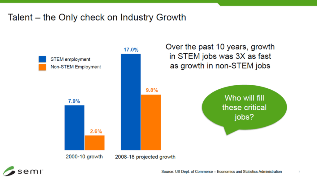
Ajit Manocha, SEMI’s president, and CEO welcomed the many attendees on Tuesday morning. Because our highly technical and rapidly changing industry needs many more workers educated in science, technology, engineering, and mathematics (STEM) fields, Manocha also highlighted a few compelling facts to encourage young people to study STEM topics. (Figure 1)
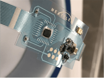
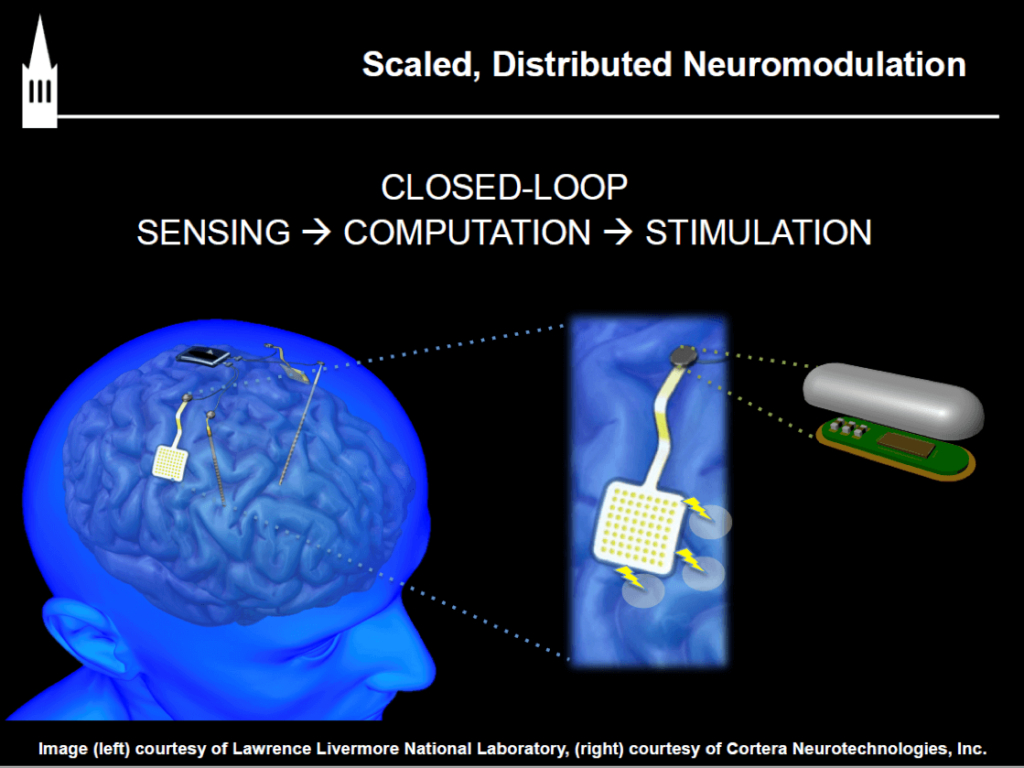
Rikky Muller, co-founder, and CTO of Cortera Neurotechnologies presented an example for impacting human lives with a minimally invasive wireless neural interface. First, she showed a movie how a quadriplegic commanded a robot arm with her brain, through a complex setup of equipment. Then Muller outlined how her company developed, in cooperation with Lawrence Livermore Labs, NovaCentrix and NextFlex, a miniaturized and wireless version of a brain-machine interface. Figure 2.
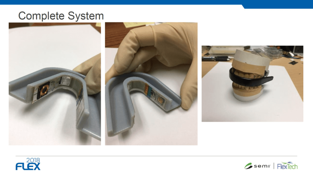
David Schwartz, the area manager at PARC, presented how his team, in cooperation with UCSD and NextFlex, developed a flexible hybrid electronics (FHE) -enabled mouth guard. They apply highly selective sensors to continuously monitor bioanalaytes from saliva, from which one might infer hydration and mental engagement levels. Schwartz stated that their results correlate better with a blood test results than with skin-patches that analyze sweat. He also described how PARC prints sensors and antennas into the mouth guard, visible in Figure 3 below.
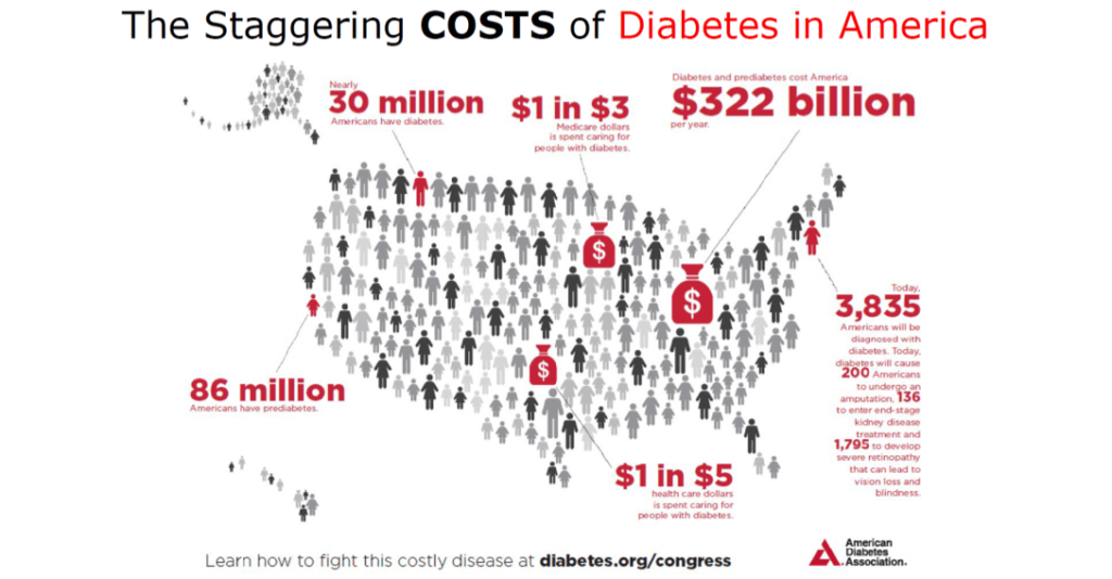
The next speaker, Lin Le, CEO of Bonbouton, surprised me when he stated that the right foot is always a few degrees warmer than the left foot. This temperature difference indicates in diabetic persons if they are likely to develop foot ulcers, which can lead to severe consequences, including amputation and death. His technology, printed into orthotics, uses graphene sensors to capture the temperatures. Because diabetes treatment consumes a major portion of the healthcare cost in the U.S.,(Figure 4) Medicare pays Bonbouton monthly fees for monitoring foot temperature differences in diabetic persons.
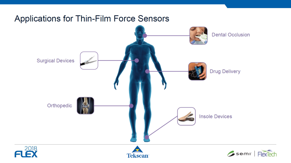
Rob Podoloff, CTO of Tekscan, presented a range of sensors that can monitor various body functions. As these printed devices are today much smaller, lighter, faster, smarter, low power and lower cost, compared to just a few years ago, body functions like pressure exerted on individual teeth, on knees and feet can be measured accurately and guide the doctors to take corrective measures. By the way, the many Dr. Scholl’s orthotics stations at Walmart and other retail outlets are utilizing Tekscan’s technology to customize insole devices to individuals.
Knowing Jan Vardaman and her in-depth packaging knowledge from many years of cooperation in the 2.5/3D-IC world, I didn’t want to miss her view of the 3D printed electronics technologies. See in Figure 6 below how TechSearch International compares traditional IC packaging with “package-free” 3D printed electronics.
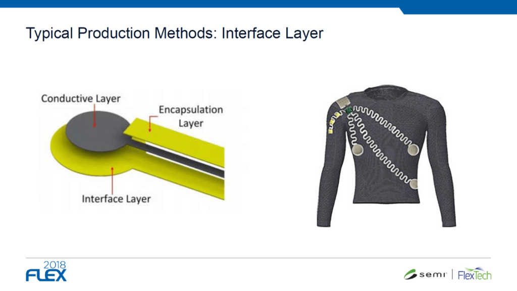
For years, there has been an ongoing discussion about how smart textiles could benefit their wearers: Monitoring fitness and/or health parameters, sensing environmental conditions to warn the wearer of potential dangers, accelerating wound healing, even adding a basic computer, including battery, to an otherwise simple sweater. Bill Babe, from LiquidX, outlined their development efforts, in cooperation with NCSU, gave several examples for practical applications and emphasized that the yarn needs to be conductive to allow printing of electronic circuits onto garments. Figure 7 shows that the conductors need to be protected, against sweat, laundry detergent, and mechanical forces to guarantee an acceptable life-span.

People who know me know that I love working on the bleeding edge of technology. It’s exciting, I learn a lot, and really enjoy opportunities where I can impact development programs in their early stages. That’s why exactly 20 years ago I started, with my team at Synopsys, a program with a young wafer foundry called TSMC. We jointly developed reference flows # 1 and 2 as well as key pieces for the first few PDKs (Process Design Kits). Both capabilities turned out to be essential for TSMC’s success and for the proliferation of the fabless IC vendor business model.
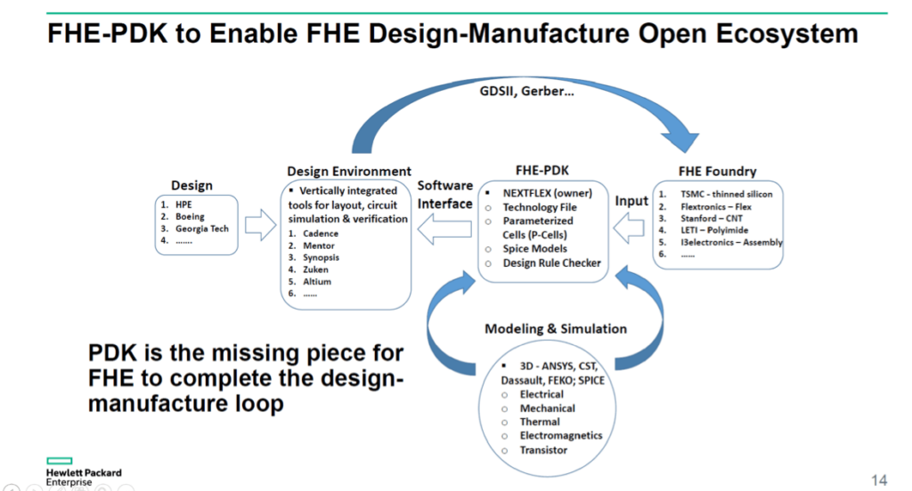
I was very happy when I saw that the FHE is industry is following this proven path. Jim Huang, Sr. Research Scientist at Hewlett Packard Enterprise, presented plans and ongoing efforts to develop, in cooperation with major industry players, a design environment for 3D printed FHEs. Figure 8 below shows how multi-faceted this program is and how many important contributors have been engaged already.
I dare to predict that this development program will become as important to the design and manufacturing of printed IoT edge nodes as well as the proliferation of a ubiquitous and intelligent IoT network as the first TSMC reference flows and PDKs turned out to become for our industry’s successful transition from the IDM business model, to the more cost-effective fabless & foundry cooperation.
To emphasize the strategic importance of this FHE-PDK, the conference organizers recognized Huang with an ALL STAR award.
Everybody who attended FLEX2018 must have noticed that the NextFlex booth was always very busy. That’s why, in addition to making FHE experts available at the conference in Monterey, NextFlex offered another opportunity to learn more about this strategically important organization. At the NextFlex Technology Hub tour in San Jose on Friday morning, Paul Semenza, Director of Commercialization, welcomed about 80 attendees and presented the plans of this public-private partnership, successes, and their broad industry support. See Figure 9. Then Semenza toured us through the facility and explained the many pieces of equipment which are available to member companies for manufacturing flow development, prototyping and low volume production.
Semenza got everybody’s full attention when he talked about a recently completed project : A printed flexible hybrid implementation of the Arduino Mini microcontroller. As an EETimes article written by Wilfried Bair describes, the FHE Arduino version is nearly 70% lighter and much smaller than the commercial Arduino Mini – a significant benefit for wearable electronics. (Figure 10).
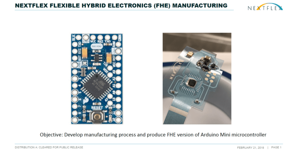
Figure 10: Before and after: hard substrate Arduino Mini and FHE equivalent, side-by-side. (Image source: Paul Semenza, Director of Commercialization at NextFlex)
If you are interested in Flexible Hybrid Electronics but couldn’t attend FLEX2018 in Monterey, you have on April 26 a convenient opportunity to hear presentations from additive process printing experts at NextFlex and well-known packaging experts at the “New Generation Flexible Hybrid Electronics” symposium sponsored by MEPTEC, and held at NextFlex in San Jose. Find conference details and register here.
3D InCites has given me many opportunities to promote packaged multi-die ICs – 2.5D, 3D and WLP – in the last several years. I hope our readership will also appreciate further news about FHE, another very promising technology! ~ Herb


