

By Abdelhamid El-Sawy, Ph.D., Senior R&D Scientist and Bud Troche, Senior Director of Wafer Level Packaging, MacDermid Alpha Electronics Solutions
Hybrid bonding is reshaping advanced packaging by enabling ultra-fine pitch copper-to-copper interconnects, essential for high-bandwidth memory (HBM), chiplet integration, and 3D heterogeneous systems. While alignment precision, oxide control, and chemical mechanical planarization (CMP) techniques have been widely studied, copper grain structure remains a less explored but equally critical factor. The way copper grains are sized and distributed forms the metallurgical foundation of hybrid bonding, enabling lower bonding temperatures, greater reliability, and stable grain structures throughout integration. The following article reviews the key challenges associated with fine grain copper. It also outlines strategies for controlling grain size to enhance bond quality, minimize voids, and reduce thermal requirements for high-volume manufacturing (HVM).
Connecting the Future with Hybrid Bonding
Hybrid bonding is an advanced 3D integration technique that directly joins copper interconnects and dielectric surfaces between stacked chips or wafers. Unlike traditional flip-chip microbump bonding, typically limited to pitches of 10–50 µm, hybrid Cu/SiO₂ (copper – silicon dioxide) bonding can achieve ultra fine pitches below 10 µm and is extending toward the submicron scale. By eliminating the need for solder bumps and underfill, hybrid bonding dramatically increases vertical interconnect density. This reduces signal delay, and lowers power loss, enabling smaller, faster, and more energy-efficient 3D packages.
First deployed in HVM for stacking Complementary Metal-Oxide-Semiconductor (CMOS) image sensor wafers, hybrid bonding has since expanded into applications such as 3D NAND memory and logic-on-memory integration, for example, AMD’s “3D V Cache”, demonstrating its value in high-bandwidth designs. The process forms planar copper-to-copper contacts embedded in a dielectric, typically SiO₂, allowing both metallic and insulating regions to bond simultaneously. This enables direct copper interconnection between dies without the need for solder, vastly increasing bandwidth and interconnect density in heterogeneous integration.
Why Hybrid Bonding Presents Unique Challenges
The industry’s push toward smaller nodes, higher bandwidth, and denser integration is accelerating the shift to hybrid bonding. While it enables sub-2 µm pitch interconnects with excellent electrical and thermal performance, large-scale adoption is constrained by several critical challenges:
- Surface Preparation and Process Control
Achieving a reliable copper-to-copper bond at fine pitch requires exceptional control over surface preparation, alignment, and process conditions. Bonding surfaces must be atomically flat, with nanometer-scale planarity and carefully controlled copper recess. - Stringent Alignment Tolerances
Accuracy within just a few nanometers is required to ensure precise pad to pad overlap. - Contaminant Sensitivity
The process must remain free of contamination. Even trace amounts of native oxide or particulate contamination can disrupt proper bonding and degrade yield. - Thermal Budget Management
Although designed to operate within a low thermal budget, moderate post-bond heating is typically needed to enhance copper diffusion and strengthen the joint - Grain Structure Control
Grain growth at low temperatures directly impacts void formation, bond strength, coefficient of thermal expansion (CTE), electromigration resistance, and overall reliability in both wafer-to-wafer (W2W) and die-to-wafer (D2W) hybrid bonding.
Recent advances in fine grain electroplating processes are addressing these barriers. Innovative chemistries are now producing ultra-pure, thermally stable, high-density metastable copper films with tightly controlled grain sizes, paving the way to higher yield and scalability.
The Role of Grain Structure in Hybrid Bonding
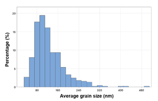
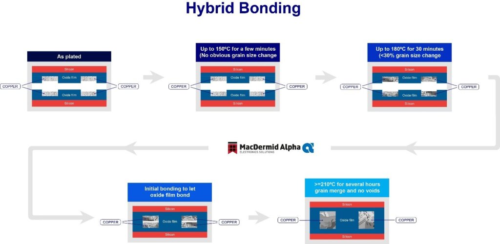
In hybrid bonding, the copper-to-copper bonds are formed through solid-state diffusion during post-bond annealing. Fine grain copper, with its high density of grain boundaries, provides significantly higher atomic diffusivity than coarse-grain structures. This enables low-temperature bonding (as low as 150°C) while maintaining joint integrity. However, metastable fine grains present challenges in process stability (Figure 1).
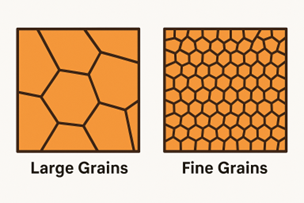
Grain sizes below 0.2 µm are classified as fine grain (Figure 2). Some applications leverage nanocrystalline copper (<100 nm) to enhance surface activity and grain boundary diffusion. While nanograins can accelerate bonding, they are often less thermally stable and prone to premature coarsening during room-temperature storage or chemical mechanical planarization (CMP).
To address these challenges, MacDermid Alpha developed grain-engineering protocols utilizing tailored additives to control nucleation, grain orientation, and growth dynamics. By tuning grain boundary energy, these methods stabilize fine grains at room temperature and enable selective grain growth during bonding, eliminating interfacial voids without over-expanding the film.
Grain Stability at Room Temperature
Fine grains naturally tend to coarsen over time, particularly when plated films are stored prior to bonding. If grain growth occurs before bonding, the bonding surface loses reactivity, forcing the use of higher bonding temperatures, further straining the thermal budget constraints, a key issue in heterogeneous integration.
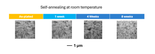
Engineered additives provide a solution by “pinning” grain boundaries, thereby stabilizing the film for days or even weeks after CMP. Studies show that grain-pinned films maintain their fine structure over extended periods, meeting integration cycle requirements for HVM.
Thermal Budget Constraints
Many hybrid bonding stacks contain temperature-sensitive layers, such as low-k dielectrics, image sensors, and CMOS circuitry, which limit post-bond annealing to below 250°C. Conventional copper films typically require temperatures above 300°C for grain coalescence, making them incompatible with these temperature restrictions. Fine grain copper overcomes this limitation by enhancing grain boundary diffusion, enabling reliable bonding at temperatures below 200°C.
The thermal budget is a critical constraint. Excessive post-bond heating can degrade sensitive device layers, cause delamination between materials with mismatched coefficients of thermal expansion (CTE) or alter the electrical properties of advanced dielectrics. Maintaining a low thermal budget preserves the integrity of the entire stack while still achieving strong, void-free copper-to-copper bonds. Striking this balance between bond quality and thermal control is essential to meeting the performance and reliability requirements of next-generation 3D integrated packages.
Coefficient of Thermal Expansion (CTE) Mismatching
Mismatch in the CTE between copper and surrounding dielectric materials can generate significant mechanical stress during bonding and post-bond cooling. These stresses often manifest as warpage across the wafer or delamination at the copper–dielectric interface, both of which undermine device reliability.
Fine grain copper helps mitigate this issue by providing greater compliance during thermal cycling. The increased density of grain boundaries enables localized plastic deformation, which helps dissipate stress and reduce the risk of interfacial damage. In fact, reducing grain size has been shown to increase the effective CTE of copper films, improving their ability to expand and conform to the opposing bonding surface. This enhanced adaptability is particularly valuable in heterogeneous stacks, where dielectric materials often have CTE values that significantly differ from copper. By accommodating these mismatches, fine grain copper minimizes stress concentrations and promotes the formation of strong, void-free copper-to-copper bonds.
Interfacial Voids and Oxidation
Interfacial voids and oxide formation are two of the most common defects in copper-to-copper hybrid bonding. Even microscopic gaps at the bond interface, can create electrical opens or high-resistance paths, undermining both performance and long-term reliability. These voids typically result from incomplete metal-to-metal contact, surface contamination, or trapped gases during bonding.
Oxidation presents an equally significant challenge. Native copper oxide forms rapidly when copper is exposed to air, often within minutes, creating a barrier layer that inhibits atomic diffusion and prevents the formation of a strong metallurgical bond. Fine grain copper helps mitigate this risk due to its increased surface energy and dense grain boundary, promoting oxide-free bonding, especially when processed in inert atmospheres such as nitrogen or vacuum.
In addition, grain-stabilizing additives preserve structure integrity and reduce oxidation after CMP, reducing defect nucleation sites. Combined, these approaches enable the formation of void-free, low-resistance, high-reliability interconnects in fine-pitch hybrid bonding applications.
Grain Engineering Protocols and Techniques
Creating fine grain copper films through electroplating requires precise control of the plating process (Figure 4). Key variables include the use of chemical additives, bath chemistry (such as pH and current density) and the electrical waveform applied during plating. By tuning these factors, it is possible to control:

- Grain size – Advanced systems are capable of tuning grain size (<0.2µm)
- Grain orientation – For example, favoring a (111) crystal texture enhances copper diffusion during bonding
- Grain boundary energy – which influences how resistant the copper is to oxidation and electromigration
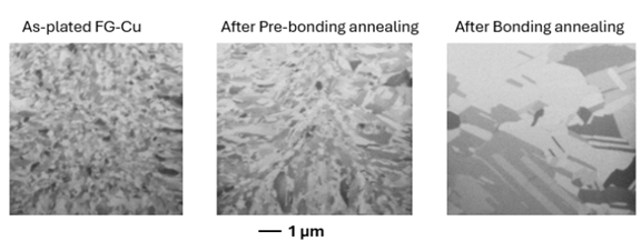
Figure 4: Thermal stability of NOVAFAB® Fine Grain Copper.
Before bonding, these films can be treated with a stress-relief anneal. This process initiates selective grain growth without allowing the entire film to coarsen prematurely. The balance between room temperature stability and activation at bonding temperatures ensures that copper films remain stable during storage, while still being highly reactive during the bonding step. This makes the process compatible with the long integration cycles of HVM.
Case Study: Hybrid Bonding for Logic-on-Memory Stacking
A logic-on-memory stack required copper interconnects at a very fine pitch (<3 µm) and bonding temperatures below 200°C. Standard copper films could not meet the necessary diffusion and yield requirements. These challenges were overcome by switching to the award-winning NOVAFAB® Fine Grain Copper electroplating process. Fine grain copper electroplating enabled bonding at lower temperatures and reduced the risk of post-bond oxide delamination. The result was a reliable, high-yield hybrid bonding solution suitable for chiplet-based architectures and scalable to high-volume manufacturing.
Performance Data with NOVAFAB Fine Grain Copper
- Average grain size: <0.2µm, confirmed by electron backscatter diffraction (EBSD)
- Thermal stability: Grain structure maintained for > 2-4 weeks at room temperature
- Bonding temperature: Reliable, void-free bonding achieved at temperatures as low as 180°C
- Shear strength: >30MPa with fine grain copper (compared to <15MPa for coarse-grain Cu)
- Electromigration resistance: More than 3x improvement over standard copper films
This case highlights how engineered fine grain copper can solve the thermal and reliability challenges of next-generation 3D packaging, especially where conventional copper films fall short (Figure 5).
Grain Engineering for Tomorrow’s 3D Stacks
Industry roadmaps predict sub-micron copper pad pitches and high-bandwidth (HBM) stacks exceeding 12 layers in the near future. At these scales, controlling copper grain behavior becomes critical. Grain engineering is expected to play a leading role in enabling:
- Low-temp wafer-to-wafer (W2W) bonding for advanced 3D logic integrations
- Die-to-wafer (D2W) bonding for AI accelerators and high-performance computing (HPC)
- Package-level integration for applications in sensors, memory, RF, and optics
Each of these integration approaches comes with unique thermal and mechanical challenges. Recent research shows that copper films can now be tailored through grain engineering to meet these diverse requirements, paving the way for reliable, high-yield hybrid bonding in next-generation systems.
Conclusion
Grain engineering has emerged as a cornerstone for the next phase of hybrid bonding. With MacDermid Alpha’s NOVAFAB Fine Grain Copper electroplating process, it is possible to precisely control grain size, orientation, and growth behavior, enabling copper metallization to meet the demanding thermal, mechanical, and reliability requirements of advanced 3D packaging. Validated for low-temperature, void-free bonding, this grain solution is helping to remove barriers to high-volume adoption.
Looking ahead, continued innovation in plating chemistry and electroplating control will further expand the capabilities of hybrid bonding. As the industry moves toward sub-micron interconnect pitches, the ability to produce copper films with highly uniform grain structures, excellent surface planarity, and resistance to premature coarsening will be essential. Improvements in additive systems and bath stability will enable closer integration with back-end-of-line (BEOL) processes and reduce variability in high-volume manufacturing.
The industry anticipates hybrid bonding at pitches below 1 µm and integration across increasingly heterogeneous materials stacks, including photonics, memory, and logic combinations. Advances in grain engineering not only reduce the required bonding temperature but also enhance thermal and electrical reliability across bonded interfaces, enabling more complex vertical architectures in advanced packaging.
Ultimately, refined copper deposition and grain-tuning technologies will unlock the next generation of chiplet and 3D IC designs, delivering greater performance, efficiency, and scalability. Continued advances in copper grain engineering will be central to enabling reliable, high-yield hybrid bonding for the next generation of 3D integrated systems.
About the Authors
 Abdelhamid El-Sawy, Ph.D., is a Senior R&D Scientist at MacDermid Alpha Electronics Solutions, specializing in advanced wafer level packaging and interconnect technologies. He develops next-generation copper electroplating processes with emphasis on grain engineering, hybrid bonding, and innovations in RDL, micro/nano TSV, and TDV. By combining materials science with process development, Dr. El-Sawy delivers high-throughput, scalable solutions that enhance performance and reliability for leading semiconductor manufacturers worldwide.
 Bud Troche serves as the Senior Director of Wafer Level Packaging at MacDermid Alpha Electronics Solutions. With over 30 years of experience in the semiconductor industry, he has held leadership roles across Product Management, Marketing, Corporate Key Account Management, and Business Development. Bud specializes in wafer level packaging, system-in-package (SiP) and advanced packaging technologies, with deep expertise in advanced interconnect solutions. He is recognized for driving innovation and delivering strategic value in complex, technology-driven markets.
Editor’s Note: This article was contributed by MacDermid Alpha Electronics Solutions. Learn more about NOVAFAB Fine Grain Copper and other hybrid bonding solutions.


