


Chip/Package Co-Design May Fulfill a Second “Moore’s Law”
Gordon Moore predicted the demise of Moore’s law and envisioned in its place larger systems built from smaller, separately packaged, interconnected systems, according to Anna Fontanelli, Monozukuri S.p.A. CEO and Founder.
Opening her presentation yesterday on innovative advanced packaging approaches during the IEEE EDAPS 2023 Hybrid Conference, at the Sugar Beach Resort, Wolmar, Flic-en-Flac, Republic of Mauritius, Ms. Fontanelli said that the semiconductor visionary accurately predicted stacked-die advanced packaging technology as the innovation successor to his own Moore’s law. She used Moore’s long-range vision to define the Advanced Packaging landscape and outlined chiplet and package co-design challenges.
Ms. Fontanelli summarized Advanced Packaging as combining different heterogeneous integration techniques, including multi-chip modules, through silicon via 2.5 and 3D integration, fan-out wafer-level packaging, system-in-package, chiplet-based integration, and/or, system dis-aggregation and re-aggregation. In other words, “everything but the chips,” she said.
“The most demanding IC systems today combine multiple components such as chiplets, memory and ASICs. The package poses the challenge of handling, updating & optimizing complex interconnects in a 3D space,” Ms. Fontanelli explained.
Present-day 3D chiplet architecture demands die stacking and silicon-to-silicon vertical communications capabilities using a mix-and-match “LEGO-like” assembly. This new chiplet packaging requires new tools, new methodologies, and new flows, she explained.
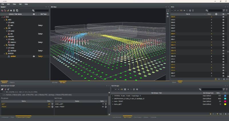
One newly available choice is MZ Technologies’ GENIOTM, the first integrated IC/Packaging EDA tool. GENIOTM is an advanced design environment integrating traditional silicon, package, and PCB design flows in one single flow. It provides capabilities for system architecture exploration, what if analysis, and I/O planning & optimization, using proprietary algorithms that efficiently map 3D interconnects.
GENIOTM doesn’t overlap with existing technologies, rather it fills the gaps left open by of the major EDA tools. To that end, new functionalities are related to timing/power/thermal analysis and physical manufacturability.

Ms. Fontanelli explained how the GENIOTM holistic design environment spans the complete 3D design ecosystem. Its co-design platform enables a revolutionary approach to integrating with physical implementation tools in both IC and package design spaces, as well as performing signal, power integrity, and pre-layout thermal estimation for physical-aware and simulation-aware system interconnect optimization.
She also revealed that on a real-design test case, GENIOTM reduced architectural design time by 60X,
About Monozukuri
Monozukuri’s mission is to conquer 2.5D & 3D design challenges for next generation electronic products by delivering innovative, ground-breaking EDA software solutions and methodologies. The technology redefines the co-design of heterogeneous microelectronic systems by providing an improved level of automation in three-dimensional interconnect optimization.


