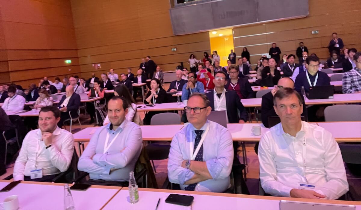
At SEMICON Europa 2023, we heard more good news about 3D heterogeneous Integration from speakers at the CEO Summit and the Advanced Packaging Conference. Not only has it become the champion for the continuation of Moore’s Law scaling, but it also allows us to deliver on power performance area and cost (PPAC) in a more environmentally friendly way. TSMC’s Doug Yu calls it scaling the “ESG Wall”. Imec’s Emily Gallagher called it achieving PPAC-E.
By now, it’s well understood and acknowledged that the semiconductor industry plays a dual role in the path to Net Zero. Semiconductor devices make possible the technology solutions needed to address climate change. However, manufacturing them has historically been a key contributor to the carbon footprint. So it’s critical to build more power-efficient solutions and 3D HI may be the way to do it.
The Sustainable System Puzzle
In his CEO summit keynote, imec’s Luc Van Den hove noted that if the semiconductor industry continues the way we have been for the next ten years, its CO2 footprint will double. Additionally, the number of wafers produced will also double. “The CO2 footprint will increase dramatically – and according to the Paris Agreement, we should be trying to half our CO2 footprint.” He called it the sustainable system puzzle. To solve it, we need to address sustainable chip manufacturing.
Van Den hove said to achieve sustainable growth, we will need advancements in both CMOS scaling and 3D integration, depending on specific workloads and requirements. He calls it CMOS 2.0 – where CMOS scaling and 3D HI will provide complimentary, system-level solutions.
Scaling The ESG Wall
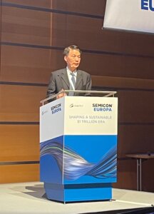
The demand for semiconductor devices to support the compute demand from generative AI applications like GPT-3 and GPT-4 is increasing, driving a need for exponential growth in semiconductor manufacturing. Yet the resulting technology is expected to be a game changer for our industry because it can be used to help us design more power-efficient 3D IC and chiplets used to build those generative AI products in the first place.
According to TSMC’s Doug Yu, the challenge to sustaining traditional Moore’s Law isn’t just scaling the “Memory Wall” or the “Power Wall”, we also now must scale the “ESG Wall”.
To deliver advanced, energy-efficient high-performance computing (HPC) to support GPT-3 and GPT-4 for example, we need enhanced systems with improved interconnect bandwidth and latency.
The answer, of course, is 3D systems solutions. But Yu cautioned that not all 3D is the same, and system PPAC isn’t more demanding than it was five years ago. He talked about TSMC’s initiatives to develop a compact photonic system leveraging 3DFabric to achieve higher integration of electronics and photonics. The result is a new series of acronyms:
- Electronic-photonic IC-ized Technology aka EPIC
- Compact Universal Photonic Engine aka COUPE
- System Technology Electronic Photonic Co-optimization” aka STEPCO.
Complexity Drives Innovation
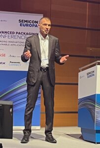
Oreste Donzella, KLA, continued along the same vein as Van Den hove, talking about how while scaling continues to evolve in the front end, HI is another way to improve performance, and it’s no longer the technology of the future. Added to that, advanced IC substrates are also enabling device performance.
Donzella explained how as an equipment supplier, KLA recognized the converging worlds of front end, back end, and substrates, as well as the increasing complexity. This led to a strategy of diversification through acquisition over the years. The company now offers complete process control solutions as well as plasma dicing capabilities for HI.
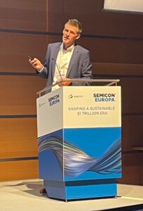 AT&S’s Markus Leitgeb continued the IC substrate story and the need for advancements in both front-end and advanced packaging technologies. He explained how advanced IC substrate technologies can contribute to providing energy and power-efficient solutions.
He explained how both core and build-up layers can be used to create a multifunctional, “Swiss Army Knife” substrate core with different advanced concepts that help solve challenges such as power delivery, interconnect density, loss reduction, and more. The most mature of these is embedded active and passive components that deliver advantages in reliability, thinner form factors, heat dissipation, miniaturization, and shorter signal paths.
The big news from AT&S is the establishment of an R&D competence center in Austria with co-development partners that will bring all the substrate building blocks together in one place. The company is looking for partners of interest for this project.
European 3D HI Pilot Line
Another exciting European project under development was co-presented by Heiko Dudek, Siemens EDA; Harald Gossner, Intel; and Michael Töpper, Fraunhofer FMD. The trio presented the case for developing a European 3D HI pilot line that will provide “a leap ahead to achieve technology leadership.”
Gossner discussed the supply chain challenges of multi-foundry sourcing. Töpper talked about the technical challenges due to the multi-physical effects of ultra-compact, miniature devices, and how they will be solved by tapping into the HI toolbox developed by Fraunhofer IZM.
In discussing design for reliability considerations, Töpper explained how digital twins make it possible to examine all the challenges posed by different materials and processes like hybrid bonding, TSVs, and integrating passive components, needed to develop high-density Si interposers. Digital twins allow for knowledge-enhanced process models for 3D HI technology chain.
Focusing on EDA tools and workflows for HI, Dudek explained that unlike ASIC designs of the past, which took an over-the-wall approach, 3D HI requires a more collaborative approach known as system technology co-optimization (STCO).
“Planning and predictive analysis is the glue that puts everything together,” he explained. “It needs a digital twin to model and predict downstream behavior.”’
Slated to be built in Q1 of 2024, this project is part of the HI Roadmaps 2030+.
Smarter Supply Chain Solutions for a Sustainable Ecosystem
Presenting on behalf of imec’s Sustainable Semiconductor Technologies and Systems initiative, Emily Gallagher steered the conversation back to the overarching topic of sustainable semiconductor manufacturing by talking about the gravity of PFAS chemicals. She introduced the new acronym I mentioned earlier – PPAC-E – and talked about the importance of measuring both operational emissions as well as embodied emissions of a chip.
To address these issues, imec recently launched imec.netzero, a bottom-up virtual fab that quantifies the footprint of a chip. Gallagher’s presentation focused on how the tool can be used to assess the IC packaging landscape to understand the role advanced packaging plays in sustainable semiconductor manufacturing. It turns out that wafer-level packaging has a significant impact on emissions adding 5% – 10% to IC chip emissions.
Thorsten vom Stein, Merck (or EMD Electronic Materials, a division of Merck KGAA Darmstadt Germany, as it’s known in the US) described efforts the company is making to advance semiconductor materials manufacturing by digitizing chemical process design. He explained that reshaping material development requires data-rich experimentation.
While he says he doesn’t expect digital labs to replace physical labs entirely, vom Stein says digitization is proving to reduce R&D cost, improve time-to-market, and reduce qualification windows. It improves the ‘first-time-right’ threshold. The goal is to move production-level data density to the very first experiment.
Can this be used to develop PFAS-free solutions? vom Stein explained that the C02 budget of the company’s process is one of the measuring parameters in the digital lab. It helps with working on abatement and coming up with surrogates for non-PFAS solutions. He also said that the company talks worth regulatory and governments to prioritize efforts the right way, but that there is a long way to go to make the dialogue more productive.
In Summary….
While this wrap-up mentions only a selection of the day’s speakers, the main messages were these: Advanced Packaging is cooler than ever, and Europe is working to build out the ecosystem to support it. Front-end manufacturing, advanced packaging, and substrate worlds are converging, and companies that recognize and support this will thrive. The entire industry is working to find solutions that reduce our carbon footprint. On the path to sustainability, it’s no longer a question of either SoC OR 3D HI, but a combination of both to achieve PPAC-E. 3D HI approaches deliver more power-efficient devices.


