
TSMC recently introduced its “3DFabric Alliance”, as part of its Open Innovation Platform (OIP), to help customers with the challenges of semiconductor and system-level design complexity. The intention is to achieve rapid design implementation for next-generation HPC and mobile applications using TSMC’s “3DFabric™ technologies.
Specifically, the company lists its goals as:
- Accelerate the 3DFabric ecosystem innovation and readiness
- Speed up 3DFabric customer adoption and production
- Lead the industry in system design by integrating advanced logic with 3DFabric technologies to provide a full spectrum of best-in-class solutions and services for semiconductor design, memory modules, substrate technology, testing, manufacturing, and packaging.
According to the company, “3D silicon stacking and advanced packaging technologies require extensive ecosystem collaboration to help designers navigate the best path through the myriad options and approaches available to them. That’s why TSMC has launched the 3DFabric Alliance. This is in addition to its existing OIP ecosystem partnership in EDA, IP, DCA, Cloud, and VCA, which offers customers an easy and flexible way to unlock the power of 3D IC in their designs using TSMC’s 3DFabric technologies, a comprehensive family of 3D silicon stacking and advanced packaging technologies.”
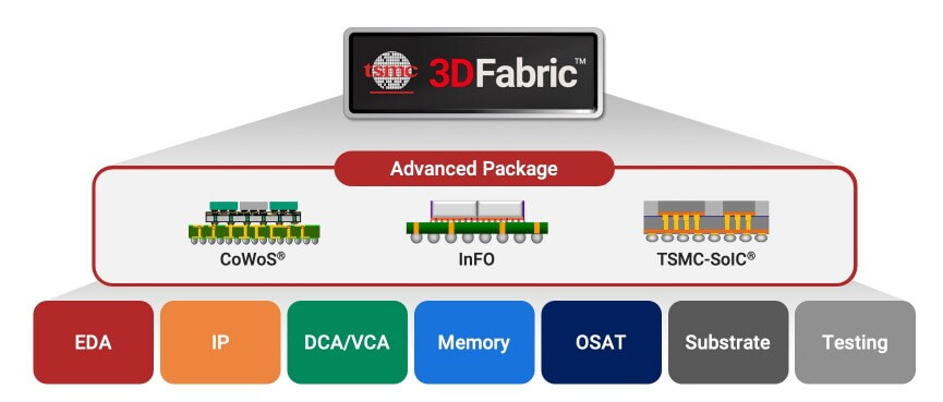
The 3DFabric Alliance will work with alliance members in the seven areas shown in Figure 1 to deliver “…solutions and services to meet customer’s 3D IC design needs in all relevant design stages of EDA tools and flows, IPs and memory components, design services, as well as backend processes including OSAT, substrate, and testing to enable customers’ delivery of quality system products.”
TSMC’s 3DFabric family of technologies consists of both 2D and 3D frontend and backend interconnect technologies. Its front-end technologies, or TSMC- System on Integrated Chips (SoIC®), use the precision and methodologies of the TSMC’s silicon fabs needed for 3D silicon stacking. These technologies include Chip-on-Wafer (CoW) and Wafer-on-Wafer (WoW) die stacking, to allow 3D stacking of both similar and dissimilar dies to deliver:
- More computing power by increasing the number of compute cores
- More memory and higher bandwidth with stacked memory
- Improved power delivery with deep trench capacitors for high-power applications
TSMC says it also has multiple dedicated backend fabs that assemble and test silicon dies – including 3D stacked dies – and process them into packaged devices.
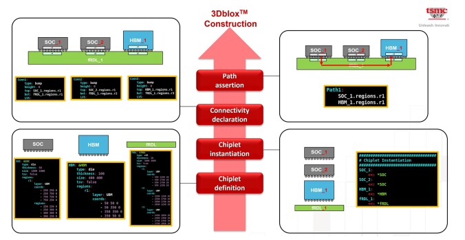
3Dblox
The 3Dblox open standard aims to modularize and streamline 3D IC design solutions for the semiconductor industry. 3Dblox is an open standard that provides generic language constructs capable of representing all current and future 3D-IC structures. It modularizes the 3D-IC structures such that EDA tools and design flow can be simpler and more efficient and ensures standardized EDA tools and design flows are compliant with TSMC 3DFabric technology.

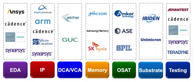
TSMC also launched the 3Dblox Committee, organized as an independent standard group, to create an industry-wide specification that enables system design with chiplets from any vendors. Working with key members including Ansys, Cadence, Siemens, and Synopsys, the committee has ten technical groups of different subjects and proposes enhancements to the specs and maintain the interoperability of EDA tools. Designers can now download the latest 3Dblox specifications from the 3dblox.org website and find more information about 3Dblox and its tool implementation by EDA partners.
Substrates
TSMC has worked successfully with substrate partners IBIDEN and UMTC to define a Substrate Design Tech file to facilitate substrate auto-routing for significant efficiency and productivity gains.
Testing
TSMC is collaborating with automatic test equipment (ATE) partners Advantest and Teradyne to solve a variety of 3D test challenges to reduce any yield loss and improve power delivery efficiency for chiplet testing. To demonstrate high-speed test access for 3D stack testing through a functional interface, TSMC is working with Synopsys and ATE partners on a silicon demonstrator to achieve the goal of a 10x testing productivity boost. The Company is also working with all design-for-test (DFT) EDA partners to ensure effective and efficient interface testing.
For all the latest on Advanced Packaging, stay linked to IFTLE……………………….


