
Jean-Marie Brunet, Vice President and General Manager of the Siemens Hardware-Assisted Verification business unit finds himself and his group in a unique situation when it comes to the topic of chiplets. The group designs a chiplet for their own products and sells those products to verification engineers who are verifying chiplet designs.
I recently had a conversation with Jean-Marie to get his perspective on chiplets and why he believes they are leading an epic chiplet evolution.
Smith: A significant challenge to chiplet adoption is scaling. Is that the biggest challenge or are there more pressing challenges?
Brunet: It’s a big topic. First, let me explain why. I manage an organization that develop hardware verification technology to the market –– emulators and FPGA prototyping hardware.
In the case of the emulator, we create all parts of the emulator. We build a very large device with a complex hardware architecture that must run a large amount of software. By developing our own hardware, we understand scaling challenges.
In terms of scaling, there is a lot of talk about how Moore’s Law is dead. No, Moore’s Law is doing just fine. Today semiconductor companies are designing for two or three nanometer process technology that uses a different type of transistor so it’s very expensive to go to an advanced node.
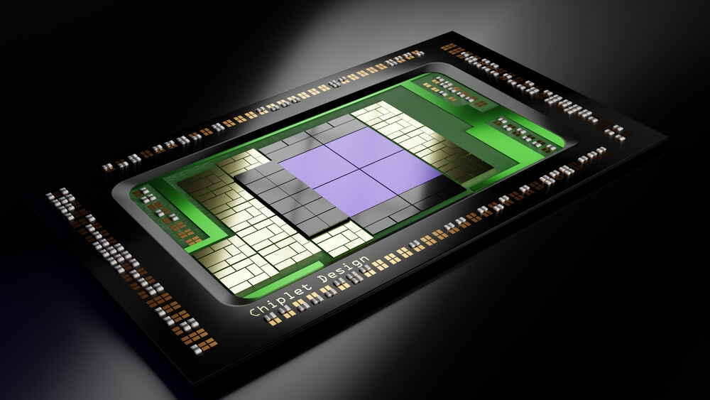
What is really happening is More than Moore. That dimension of system scaling is where the chiplet plays a role — this is an incredible opportunity to design a complex system that allows mixing and matching functionality that is not simply logic devices. For example, they could be logic, memory and/or analog. With chiplets, you can integrate different functions from different processes. You can choose between either a 2.5D integration with a silicon interposer or 3D if you want to go all the way to solving complex challenges with chiplets as a cluster and scaling architecture. The options are More than Moore and Moore’s Law or a combination of both. Companies are better equipped today than 20 years ago when there were no choices. It was only Moore’s Law.
What is relevant is when you do large devices, you have some limitations on how far you move the boundary or the envelope of what you’re trying to do. Most of the large devices in the world today are using More than Moore. Designers are using a complex package or a silicon interposer to connect different types of devices, sometimes memory and logic or they are going to chiplets. We see the Universal Chiplet Interconnect Express (UCIe) emerging as a viable direction for chiplet technology and an evolution to connect different chiplets to and architect a system.
At ISSCC in 2021, Sam Naffziger, AMD senior vice president, corporate Fellow, and product technology architect, described AMD’s EPYC chiplet evolution, comparing a traditional monolithic single device in a large package against a chiplet-based system using a clever type of stacking and chiplet technology. The chiplet solution proved to be lower cost and provided better performance and lower power than the monolithic chip solution.
Smith: Let’s talk about the verification environment. You explained that chiplet design or heterogeneous integration could include analog and RF digital memory. Does today’s verification environment support this? If not, what is missing and what needs to be done to support it?
Brunet: It’s already a requirement to validate and verify this type of system. The notion of verifying a system with multiple SoCs on the board from a methodology perspective is similar to doing a chiplet except the boundary of the SoC is different. You instantiate multiple chips and have a fabric that interconnects those chiplets. From the high-level technology, it is similar to verifying multiple sources on the system. It’s not as easy as I describe it though because it’s a challenge of fabric, interconnect, and capacity.
At some point when looking at a chiplet, the fundamental problem is size. You wouldn’t go this technology path if you’re not trying to adapt to a design that is extremely big. The problem is the ability to scale in capacity. Not every emulator is able to scale equivalently in capacity. It’s a capacity scaling challenge and it’s binary. Either you can or you cannot.
If you have to verify a chiplet implementation that encompasses 10- to 12-billion gates (probably the largest design in production), you have a binary verification validation checkpoint to pass that is, “can I emulate that?” “Is my hardware and methodology built to scale to that size?” If the answer is yes, it means you have an environment that allows you to compile and run something that is at the size of 10-billion gates. If the answer is no, then you have to modify your methodology to accommodate the maximum size allowed by emulation.

Smith: Backing up a level to the general question of design, what other kinds of challenges and opportunities are there in helping designers move to chiplet-based designs?
Brunet: If you really understand well when you architect your chip that the physical implementation is going the chiplet route, there is work that needs to be done early on. You target your design and your architecture to accommodate. It’s not like you know you’re doing an IC then suddenly move to chiplet. You can’t do that, and this is where planning comes in. For example, when people say I will do universal verification methodology (UVM) acceleration, you cannot do UVM acceleration without modifying your environment to be UVM-friendly. It’s similar. You cannot decide to go to a chiplet because of a capacity problem. The planning needs to be done at the architectural level.
Still, you always have the debate on when to choose a large monolithic device. The yield is low because the device is very large even though the device testing is relatively straightforward. With a chiplet and a multi-die architecture, how do you manage test effectively? Academic studies show that you can actually get better yield if you develop the test architecture along with the chiplet implementation. If you are interested in more information on this topic, I recommend you to look further at an Siemens offering called Tessent SSN.
To answer your question, there are clearly challenges with implementing chiplet-based designs. You don’t want to go there blindly and figure it out along the way.
Smith: What are your thoughts on the market or how the markets going to evolve?
Brunet: I’m going to answer differently than what you expect. How can I say that this is so advanced and so different and unique than what we have been doing for the past 10 to 15 years and that it will enable fantastic innovation?
If you look now, among all the large or the largest device out there, some are large FPGAs, some are big CPUs and some are GPUs or custom accelerators. All of them are implemented in 2.5 D or 3D. If anybody tells you this is a monolithic device at that size, that is not the case even though they all may use different approaches and technologies.
This is where the innovation is. The differentiated (confidential secret) is how everybody’s doing a little different flavor of the implementation to gain competitive advantage. That is why it is going to be a challenge to go toward standardization. The big discussion is about UCIe as a way to standardize. This has merit for the industry, and we are supporting it.
Smith: The chiplet evolution is the thing now. What do you see happening beyond chiplets? Or is there a beyond chiplets?
Brunet: I think we are going to have the chiplet architecture for a long time because the combination of More than Moore, advanced packaging, system scaling, chiplets and Moore’s Law allows companies to develop new and more complex products than are feasible using the older monolithic approach.
It’s an epic chiplet evolution.