Advances in packaging can improve yield and reduce cost. Can they also reduce the environmental footprint of an electronic device?
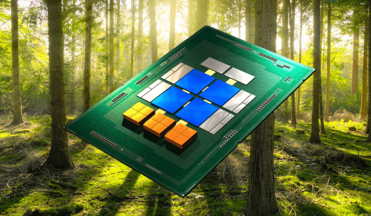
Let’s consider one example, the chiplet. Instead of large-monolithic CPUs with multiple functions integrated into one piece of silicon, the functions are divided between multiple smaller chiplets mounted on an organic or silicon substrate. Proponents of chiplets talk about the many benefits of chiplet-based designs—yield improvements, power reduction, and design flexibility.
I am not hearing much talk about environmental sustainability in discussions about chiplets. But there is a sustainability story behind each of the benefits in the previous paragraph.
Yield Improvements
Yield will generally be higher for multiple smaller dies than for one large die. Higher yields translate to less scrap silicon. Silicon is an energy-intensive material to produce. Then there are all the process chemicals, functional layers, and energy that goes into manufacturing a wafer. Yield loss means that all those resources go to waste.
It will not be possible to reduce defects to zero, but it is less wasteful to discard one defective chiplet than to scrap an entire monolithic CPU. Waste has both financial and environmental costs.
Power Reduction
Discussions about sustainability in the semiconductor industry often focus on energy consumption. Actions to keep energy consumption in check have been successful. For example, energy consumption from data centers grew only 6% from 2010 to 2018, while storage capacity increased 25x.
There is still plenty of opportunities to reduce energy consumption for a given level of performance, and chiplet designs are one way to do that. Performance, however, is critical. As Francoise mentioned in an article on chiplets, “No new technology is adopted until there is no other way to achieve performance goals.” Modular designs like chiplets seem like a path to optimizing yield and power consumption while improving performance.
Design Flexibility of Chiplets
With the announcement of the Universal Chiplet Interconnect Express (UCIe) standard, 2022 might be the year of the chiplet. This is an open industry standard, which is good news for design flexibility and innovation.
The standard promotes the interoperability of chiplets from different manufacturers. That can help with sourcing and might give packaging houses more options to support local suppliers or those with stronger environmental credentials.
Chiplet manufacturers can group similar chiplets on one wafer to improve production efficiency. If those chiplets all require the same number of lithography steps, producing several different chiplets in parallel streamlines operations. It can reduce the total energy and resources required to produce all the chiplets needed for a system.
Designers can choose the ideal process node for each chiplet. Compute cores may need the most advanced nodes available. Memory and I/O functions can use legacy nodes. A chiplet approach makes it easier to make deliberate choices about process technology. If those choices result in overall yield or energy efficiency improvements, those improve the environmental footprint of production and operation.
The UCIe standard offers packaging options depending on whether the designer wants to prioritize cost-effective or power-efficient performance. That could make it easier to choose different solutions for different end markets.
Open collaborations like UCIe are essential to advance sustainability. I realize that environmental impact was not what drove leaders in the industry to form the UCIe, but it can still stand as an example of the need to work together. We need pre-competitive collaboration to find solutions that allow the entire industry to progress.