
Technical papers to highlight the breakthrough capabilities of EVG’s LITHOSCALE® maskless lithography solution and OmniSpray® resist coating technology for “More than Moore” applications
EV Group (EVG), a leading supplier of wafer bonding and lithography equipment for the MEMS, nanotechnology and semiconductor markets, today announced that new developments in heterogeneous integration and wafer-level packaging enabled by its advanced lithography solutions will be highlighted in several papers being presented at the 2022 IEEE 72nd Electronic Components and Technology Conference (ECTC), to be held May 31-June 3 in San Diego, Calif.
- “Lossless High-speed Silicon Photonic MZI Switch with a Micro-Transfer-Printed III-V Amplifier” (Session 10, Novel Photonics Packaging Technology – Wed., June 1, 4:45pm)*
This joint paper by EVG, imec, the Photonics Research Group and the Tyndall National Institute, describes a novel approach for integrating III-V components on an advanced silicon photonics (SiPh) wafer through micro-transfer printing—enabling the economical and scalable integration of optical gain elements in photonic integrated circuits without modifying the established SiPh flow. To enable micro-transfer printing, an ultrathin bonding layer is applied to the source wafer by spray coating using EVG’s proprietary OmniSpray® technology, which provides excellent uniformity results on challenging topographies.
*This presented work is part of the CALADAN Project, an initiative of the Photonics Public Private Partnership (PPP), supported by the European Union’s Horizon 2020 Innovation Program under grant agreement No 825453.

- “Optimization of PI and PBO Layers Lithography Process for High-Density Fan-Out Wafer Level Packaging and Next Generation Heterogeneous Integration Applications Employing Digitally Driven Maskless Lithography” (Session 34, Processing Enhancements in Fan-Out and Heterogeneous Integration – Fri., June 3, 1:55 pm)
This joint paper by EVG and Fujifilm Electronic Materials evaluates high-performance dielectric materials tailored for fan-out wafer-level packaging (FOWLP) using EVG’s novel LITHOSCALE® maskless exposure lithography system, which allows for design flexibility and instant application of bias/offsets and optical proximity corrections at the die- and wafer-level. The ability to enable instant design alteration enhances final process results, such as resolution, via footing and side-wall profile, while the mask-free approach of LITHOSCALE avoids yield issues associated with reticle stitching when patterning larger-area dies.
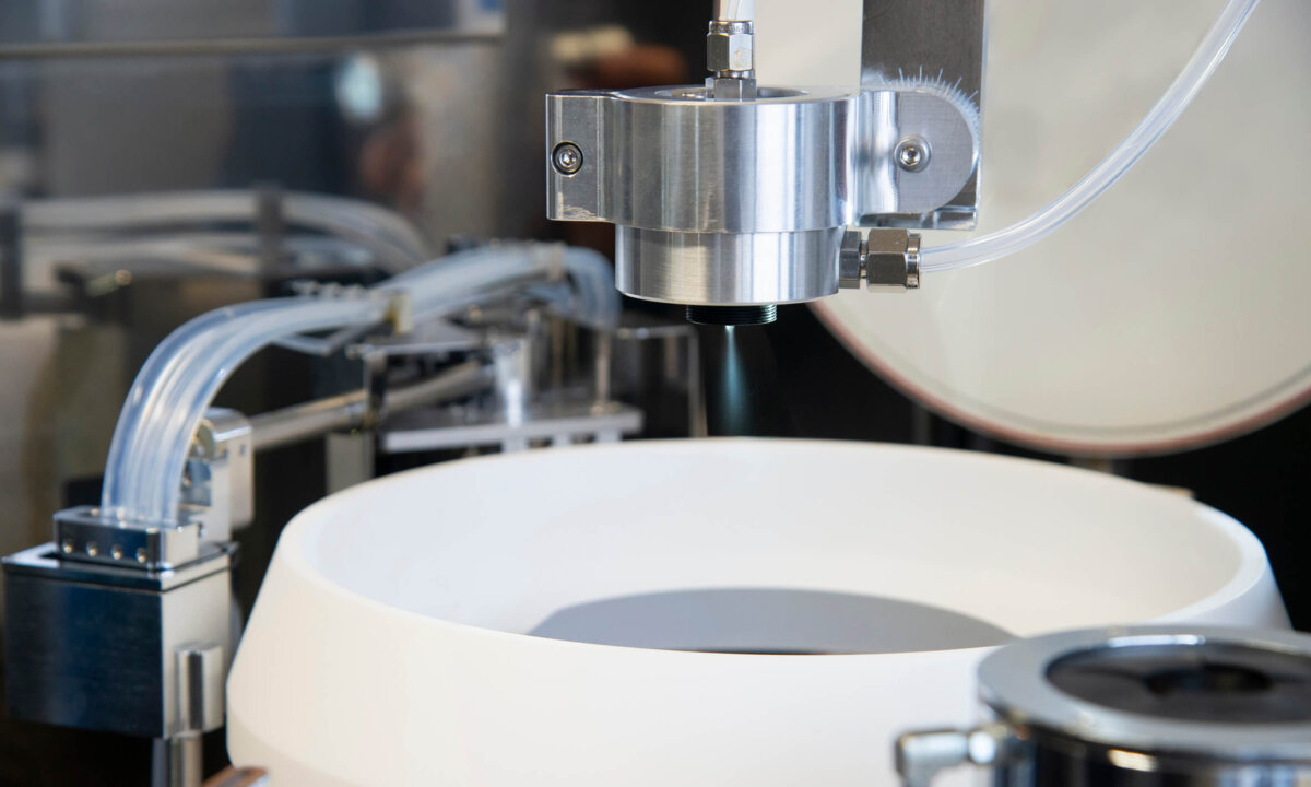
Pictured above, the LITHOSCALE® maskless exposure system from EV Group brings the benefits of digital lithography to high-volume manufacturing. LITHOSCALE eliminates mask-related consumables with its mask-free approach, while its tunable solid-state laser exposure source is designed for high redundancy and long life-time stability with virtually no maintenance and no re-calibration required.

EVG’s wafer bonding, lithography, and metrology solutions enable the development and high-volume manufacturing of technology innovations in advanced packaging—including backside-illuminated CMOS image sensors and other 3D-IC stacked devices—as well as in MEMS and compound semiconductors, such as SiPh and engineered substrates. Recent breakthroughs in wafer-to-wafer and die-to-wafer hybrid bonding to address the needs for 3D device integration, wafer bond alignment technology to address future 3D-IC packaging requirements, fusion bonding for front-end-of-line layer transfer processes, maskless exposure for FOWLP, and nanoimprint lithography (NIL) to support wafer-level optics (WLO) manufacturing, are just a few examples of EVG’s technology leadership in heterogeneous integration and wafer-level packaging.
In addition, EVG engages with companies and research groups across the technology supply chain to develop high-volume manufacturing solutions that drive new innovations in semiconductors, sensors and photonics for a wide variety of automotive, industrial, and home entertainment applications.
ECTC attendees interested in learning more about EVG and its suite of wafer bonding, lithography and metrology solutions for heterogeneous integration and wafer-level packaging are invited to visit EVG at booth #602 on May 31-June 3 at The Sheraton San Diego Hotel and Marina in San Diego.


